13E1 STEAMPUNK POWER AMP
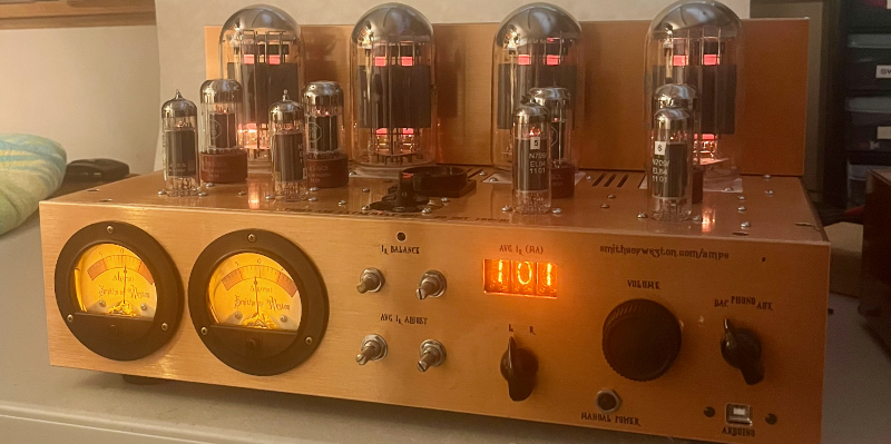
This is my most recent last amplifier project ever. I bought 4 fabulous 13E1 tubes, mainly because they are beautiful. I think they were originally intended as transmitting tubes, but are now used primarily as audio amplifying tubes. When fully running, they have a wondrous glow, evoking a simpler, much larger carbon footprint era. I love it.
POWER STAGE
This will be another push-pull amplifier, with the tubes used in tetrode mode, with a regulated 250V on the screen grid. There will be around 12.5% cathode feedback derived from the output transformer, which will have to be fairly complex - I have learned to design and wind my own transformers and chokes so I will be custom building the output transformers; the agonizing process can be found in the transformers section of this website. I will also design and wind my own power transformers and chokes. These will be built by Smith Iron, a just-now formed subsidiary of Smith Amps, lol.
The maximum anode dissipation of a 13E1 power tube is 90W. With 500V and 110ma on the anode, each 13E1 will drop about 55W just to operate, which is less than 70% of max Pa. 56W X 4 = 224W of delicious room-heating wasted power.
Below is the output stage for a single channel. There is close to 500V DC on the anode of each 13E1. Cathode feedback (CFB) is derived from the output transformer and applied to the cathodes of each power tube. The amp was driven to just before clipping and the numbers are shown on the schematic.
The input to the 13E1 push-pull circuit is 135Vrms (67.5V X 2) and the output is 582Vrms. The cathode feedback is 39.5Vrms applied to each cathode. As a check on the competence of my transformer winding, 39.5 / 291 = 13.5% which is pretty close to 12.5%, which was the design goal. So the gain of this stage without CFB is A = 291 / (67.5 - 39.5) = 10.4, and with CFB, A' = 291 / 67.5 = 4.3.
Another check on my transformer winding: the voltage ratio is 582 / 19.8 = 29.4, so the impedance ratio is the square of this, 864. The reflected impedance (Ra-a) = 8 * 864 = 6.9K, which is reasonably close to what was predicted - see the transformer section below.
There will be further global feedback applied after the circuit is built. At setup calibration, voltage across the 1R resistors will be measured with a voltmeter to determine Ik1 and Ik2. Vk1 and Vk2 are measured with the voltmeter. Now the total resistance from cathode to ground can be calculated as Vk / Ik = Rtotal. The Teensy is set up to measure Vk1 and Vk2, and it will use Rtotal to calculate Ik for each channel.
The circuitry to the left of the output stage provides the bias voltage to the grids. The 10K potentiometer R2 is located on the front panel and is adjusted to keep the cathode currents equal as displayed on the front panel by the large meters. The 10K potentiometer R1 is also located on the front panel and is adjusted to keep the cathode current at a given level, as displayed by the retro nixie tube display on the front panel. There are a total of 4 pots on the front panel for the 2 channels.
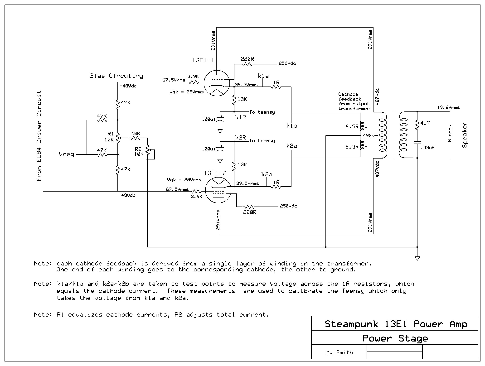
The maximum allowed dissipation power for each tube is 90W. I will use 70% of that to increase longevity - so around 63W. With 450V on the anode, a reasonable anode current (Ia) = 63 / 450 = 140ma. So I'll use around 120ma to be kind to the tubes. This value is obtained by adjusting potentiometer R2, and the anode currents of each 13E1 of the pair will be equalized with potentiometer R1.
DRIVER CIRCUITS
The circuit for one channel is shown below. All voltage and current values were directly measured with the circuit in operation at near clipping.
The input circuit is a standard long-tailed pair (LTP) made up of my favorite super-linear small-signal triode, the 6SN7. Each tube comes with a pair of triodes, and I have paralleled them. The standard cathode resistor is replaced with a constant-current source (CCS, described below) to achieve maximum linearity. The CCS is set at approximately 15.6ma, which means that an absolutely constant 7.8ma will flow through each 6SN7 triode pair. The 6SN7 anode resistor is 19.5K (2 39K resistors in parallel) so will drop about 148V, leaving 150-160V on the anode. Plotting Vanode and 3.9ma on the characteristic curves of the 6SN7 (see below, red dot is operating point) looks like a pretty linear region. Because the current at the anode can never change, no matter what AC voltage is there, this means that the effective anode resistance Ra is infinity (to AC voltages). So the gain of the circuit is mu, which is about 16.
The actual gain is A = 14.3. After GNF (global negative feedback) is applied, the gain A' = 5.23.
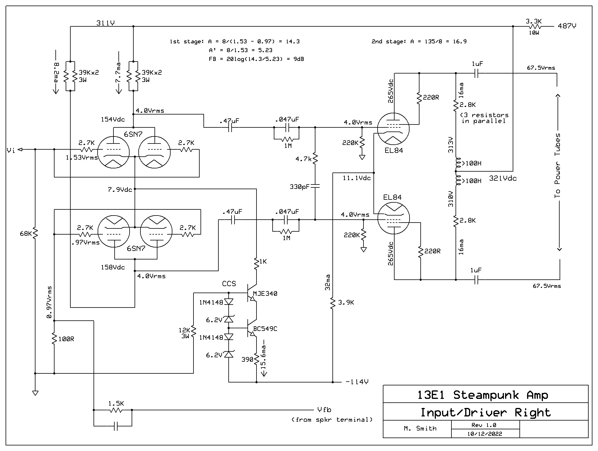
The CCS's are placed on a printed circuit board with some other circuits, discussed below.
The 1N4148 diodes are placed in the circuit to counteract temperature-induced changes in transistor Vbe's - presumably the same changes will occur in the n-p junction of the diode and cancel out those in the transistor. Is this really important? Probably not. The voltage drop across the diode is about the same as the Vbe, so we're left with Vr = Vz or about 6.2V. To get 16ma, R needs to be about 6.2/16 = about 390. The MJE340 transistor has to be heat-sinked.
Feedback (Vfb) is applied to the grids of the lower tubes in the LTP. The feedback fraction is set by Rf and the 100R resistor. Note that the feedback signal must be in phase with the input signal. If not, positive feedback and oscillation. Rfb will be determined empirically once the amp is built. It is discussed in the feedback section later on.
EL84 DRIVER STAGE
The EL84 driver stage is seen to the right in the above diagram. Patrick Turner (RIP) was a big proponent of the EL84, particularly in circuits that use cathode feedback (discussed later). This is because cathode feedback raises the RMS Vk of the power tube significantly, so to get sufficient Vgk to drive the power tubes, you need a significantly higher Vg, and this means you need big driver tubes to provide those high voltages to the power tube grids.
A few calculations: Vo into 8ohms at clipping is around 19.8Vrms (49W). To achieve this, you can see from the diagram that the pair of EL84's need to push 135V into the push-pull 13E1 circuit.
In order to get higher voltages without a high rail voltage, Turner likes to choke load the EL84 anodes. This is an old school approach, and the amp would probably be fine without choke loading, but I just learned to design and wind transformers and chokes, so what the hell. A choke allows the anode voltage to swing higher than the rail voltage, which is a useful feature. Another advantage is that these chokes can survive many of my building screwups, as opposed to somewhat frail CCS circuits. An interesting note is that each choke is wound with 2115 meters of 32AWG wire. That's right - over 1.3 miles of wire per choke, so the choke resistance is over 1100 ohms. The design of the choke can be seen here.
Note the large inductance in the anode chokes. The 2 chokes are wound on the same bobbin with the same core. They are center tapped, so half of the DC current goes one direction, the other half goes the other direction. If the two currents are equal, the core sees a DC current of zero, and will not saturate, so theoretically no gap is needed. This requires serious tube matching, so I went to my favorite supplier, Jim McShane of McShane Design and he provided me with a closely matched quad of EL84's.
To confirm the match, I used my favorite tool, the uTracer3 and generated the following curves. They are indistinguishable from one another! With 250V on the anode and screen (triode mode) and Vg = -10, each tube produces exactly 20ma of anode current. So, there should be minimal DC current through the anode chokes if I set everything up correctly.
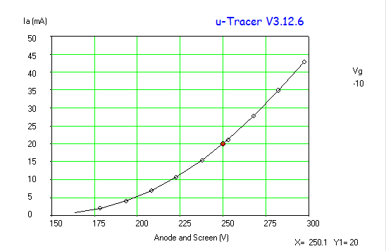
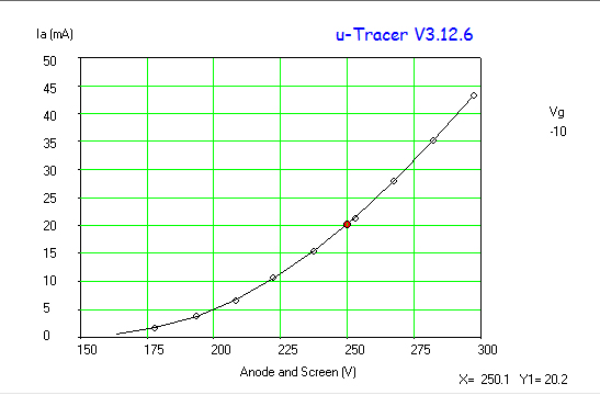
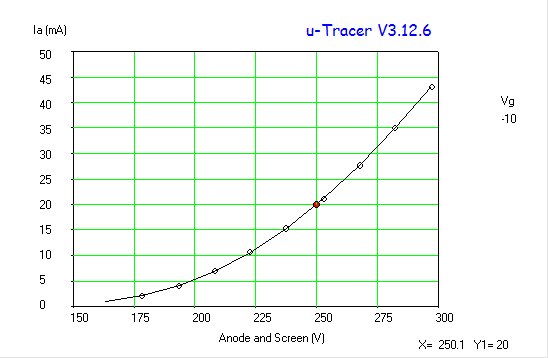
I am not going to gap the chokes. At 1kHz, the impedance presented by each choke is at least 2*pi*1000*100 = 628K, and at higher frequencies, in the megaohms.
OUTPUT TRANSFORMERS
The output transformers were designed by me - with a LOT of guidance from Patrick Turner. The gory details of their design and construction can be seen on the transformers page here. The design of these transformers is old-school and they should rival the best transformers in the world, namely the multi-thousand dollar transformers from Tango, Lundahl, and others.
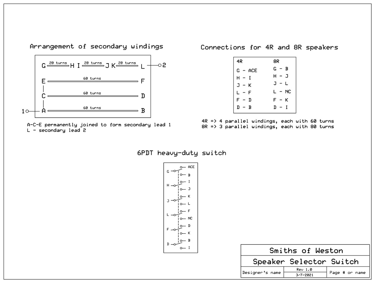
My output transformers are extensively interleaved and are shown in schematic fashion below. This method of displaying the winding diagram is directly lifted from Patrick Turner, may he RIP.
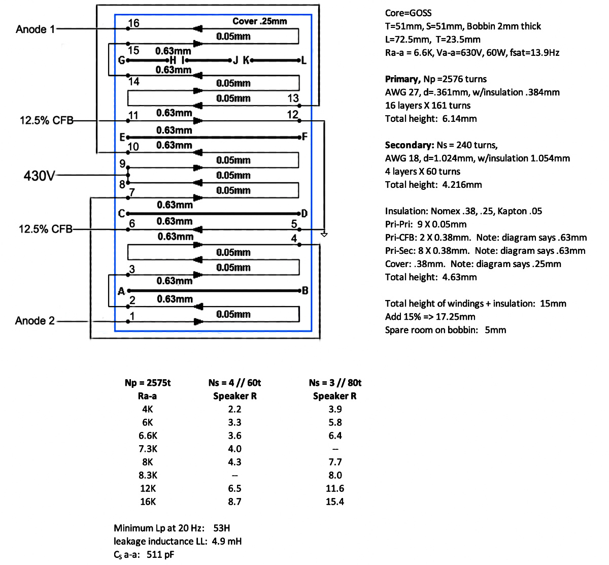
Each of the horizontal line segments represents a layer of winding and the arrows indicate the direction of winding. The thin lines are primary windings and the thick lines are secondary windings.
The deepest secondary winding has wires coming out of the transformer labeled A and B. The next layer of secondary winding is C and D, followed by E and F. The top layer of secondary windings is divided into 3 portions each having 20 turns. If you just connect A,C,E, and G on one side and B,D,F, and L on the other side, and then connect G-H, I-J, and K-L together, you get 4 windings of 60 turns in parallel. So your secondary is equivalent to a very thick wire with 60 turns. This is the arrangement for a 4 ohm speaker
OTOH, if you hook B to G, and hook D to I, and hook F to K, you now have 3 secondaries, each with 80 turns. Now parallel the 3, and you have the equivalent of a thick wire of 80 turns. This is the arrangement for an 8 ohm speaker. At the bottom of the diagram, calculations are made. If you have secondary of 60 turns, and hook to a 4 ohm speaker, Ra-a calculates to 7.3K. Likewise, if the secondaries are connected for an 8 ohm speaker, and you connect to an 8 ohm speaker, you get Ra-a of about 8.3K. This is all close enough. Speakers are never even remotely close to whatever impedance they are rated at.
These arrangements can be accomplished with a big switch. I am so proud of this design, I feel compelled to show it again below, lol. The amplifier will need two switches, one for each channel, and they are huge, to handle the large currents.
FEEDBACK
CATHODE FEEDBACK
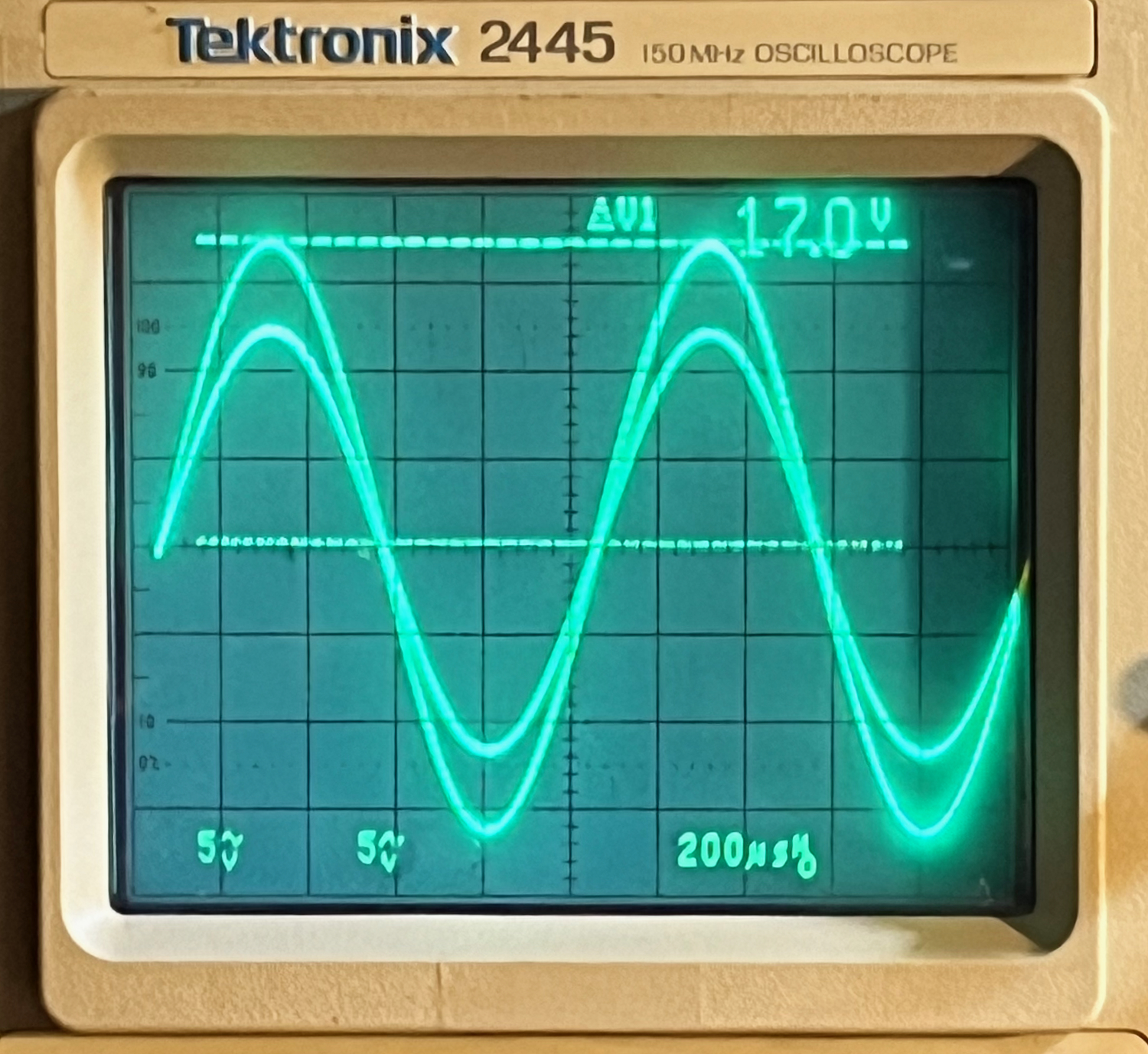
As described above, I wound the output transformers with two windings each for cathode feedback. The image below shows the effects of cathode feedback. The larger (17Vp) tracing is the voltage applied to the grid of one of the 13E1's on the right channel. The smaller tracing (around 12V) is the voltage from the cathode feedback winding applied to the cathode. With no CFB, the cathode is grounded (almost) so Vgk = 17V - 0V = 17Vp. With CFB, 12V is applied to the cathode, so Vgk' = 17 - 12 = 5Vp.
It can be shown that feedback = 20log(Vgk'/Vgk), so cathode feedback = 20log(5/17) = -10.6dB.
GLOBAL NEGATIVE FEEDBACK (GNF)
Patrick Turner used only 8dB of global negative feedback (GNF), and I will stick with that number. This is standard GNF, taken off the speaker terminal and fed back to the input 6SN7 differential amplifier through a feedback resistor Rfb. See the Driver Circuit schematic above.
There is a compensation capacitor in parallel with the Rfb - more on this later. A 100ohm resistor is then taken to ground, to make a voltage divider.
RIGHT CHANNEL
With the speaker set at 8 ohms, and an 8-ohm dummy load, the open loop gain A=40. Open loop gain is gain without GNF.
With the speaker set at 4 ohms and a 4-ohm dummy load, the open loop gain A=29.
Using my handy-dandy Excel spreadsheet, to get a GNF of 8dB, I calculate that the feedback resistor is R = 2546 on the 8R setting, and R=1818 on the 4R setting. A 1.8K resistor should work fine for both.
With this 1.8K resistor, the following are predicted:
8 ohm: A = 40, A' = 12.88, GNF = 9.8dB.
4 ohm: A = 29, A' = 11.48, GNF = 8.0dB
LEFT CHANNEL
With the speaker set at 8 ohms, and an 8-ohm dummy load, the open loop gain A=40.
With the speaker set at 4 ohms and a 4-ohm dummy load, the open loop gain A=29.
With a 1.8K feedback resistor like the one on the right channel, you get:
8 ohm: A=40, A' = 12.88, GNF = 9.8dB.
4 ohm: A=29, A' = 11.48, GNF = 8.0dB.
COMPENSATION NETWORKS
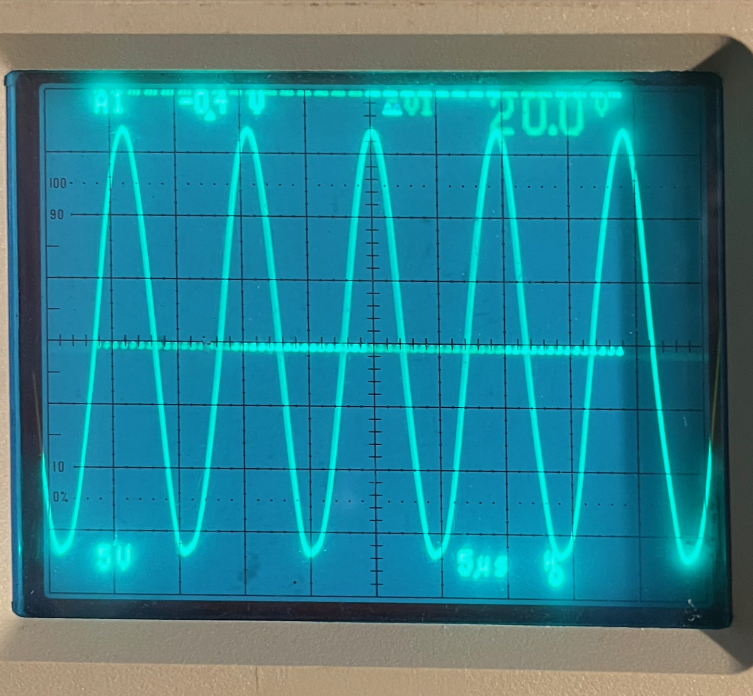
The major problem with global negative feedback is the very real risk of oscillation. To demonstrate it, I hooked the speaker terminals to a pure capacitive load (.47uF) and got the beautiful sine wave below. Note that the wavelength is almost exactly 10 usec, so this is a 100 kHz sine wave at about 17V! That is a speaker killer. This needs to be brought under control.
The idea is to kill high-frequency signals. The first place is at the feedback resistor (see Driver Circuit schematic above). A capacitor is placed parallel with the feedback resistor. At high frequencies, the capacitor's impedance is very low, so it effectively shorts out the feedback resistor, greatly increasing feedback at high frequencies.
Another network is placed at the input to the EL84's - this is a 4.7K resistor and a 330pF capacitor.
Finally, a Zobel network is placed at the output of the amplifier, just before the speakers. This is seen on the Power Stage schematic and consists of a 4.7 ohm resistor and a .33uF capacitor.
The only one of these that really did the job was the Zobel network at the output, and it killed the oscillation even with a pure capacitive load from .01uF to 2.2uF. The amplifier should be unconditionally stable.
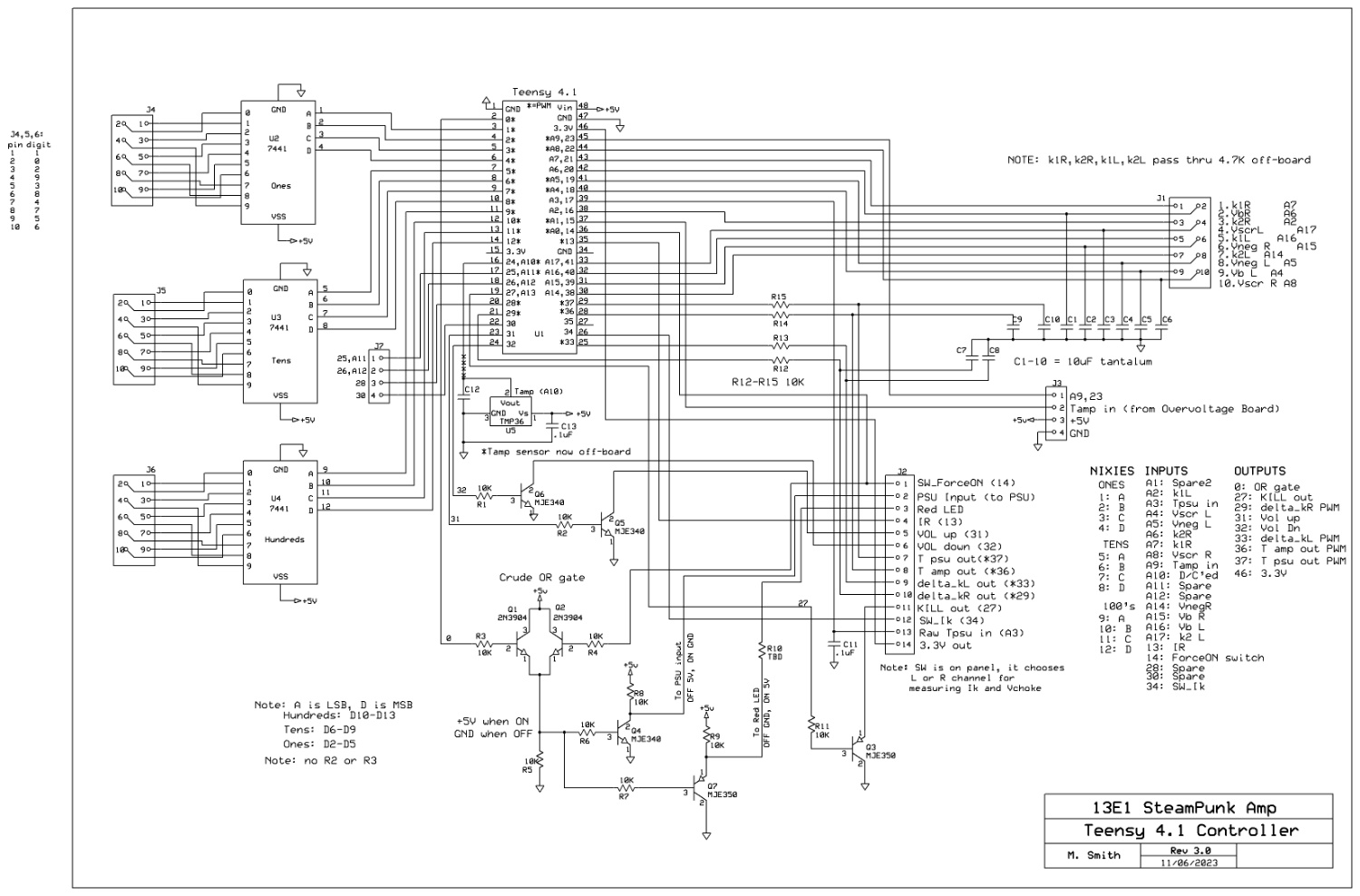
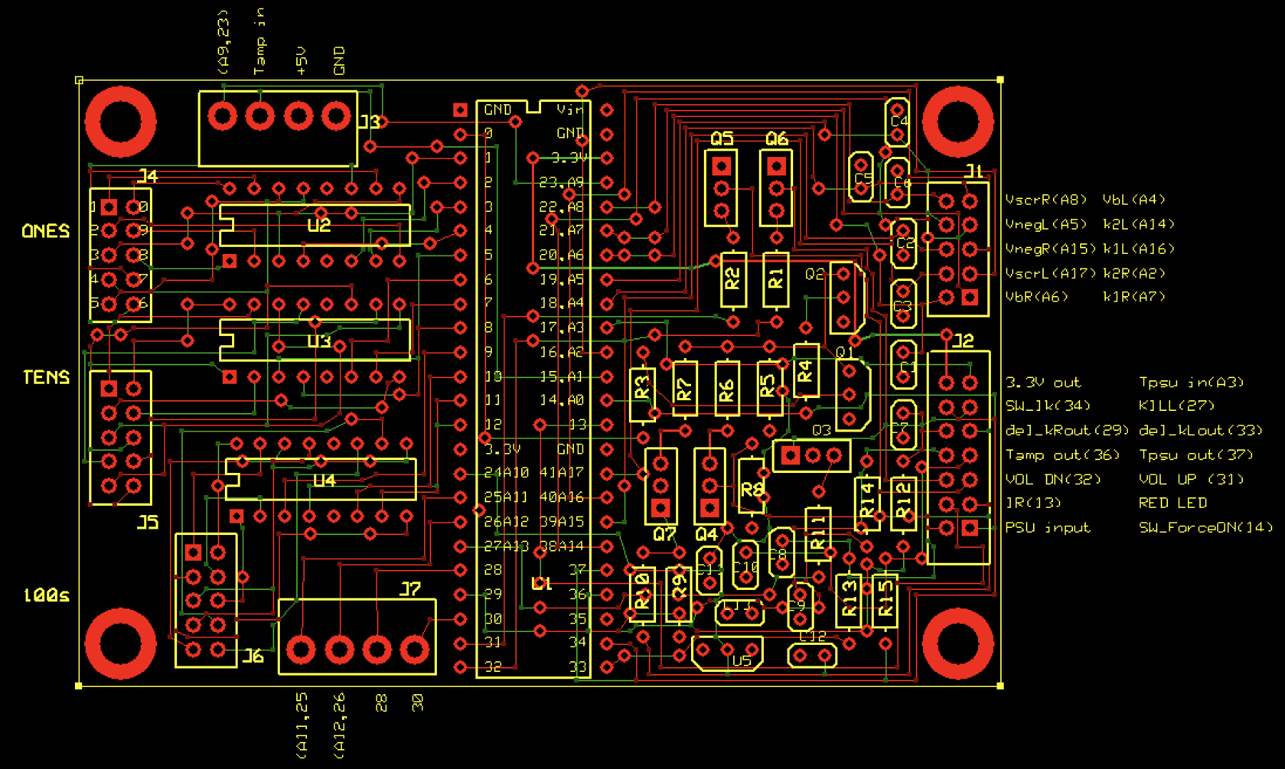
TEENSY 4.1 MICROCONTROLLER CIRCUIT
I am using mostly analog meters customized with SmithsofWeston faceplates, and some very old-fashioned Nixie tubes. In order to sample all the voltages, currents, temperatures, etc. to display on the meters, I am using a rather more modern approach. I use a microcontroller which I have programmed to carry out all these functions.
The schematic is shown below. I am using the awesome Teensy 4.1 microcontroller, which works just like an Arduino, but is much smaller and has far more I/O ports. It is a 2 sided integrated circuit, but I will only be using the top side, because that will provide me with enough I/O ports. It will drive the Nixie tubes via the antique 7441 nixie drivers. J1 receives all the voltage and current information from the "Overvoltage/CCS" board described below and sends it to the Teensy. J2 is mostly output to the meters, but it also inputs the digital output from the IR receiver. Input from the thermometers also arrives via J2, as well as 2 switches. The KILL signal to the PSU outputs through J2. The control signals to the volume potentiometer exit via J2.
The circuit at the bottom of the schematic is a simple OR gate. It outputs a LOGIC1 if either the manual on-off switch (J2-pin1) is pushed or if the Teensy (activated by the remote) sends a turn-on signal.
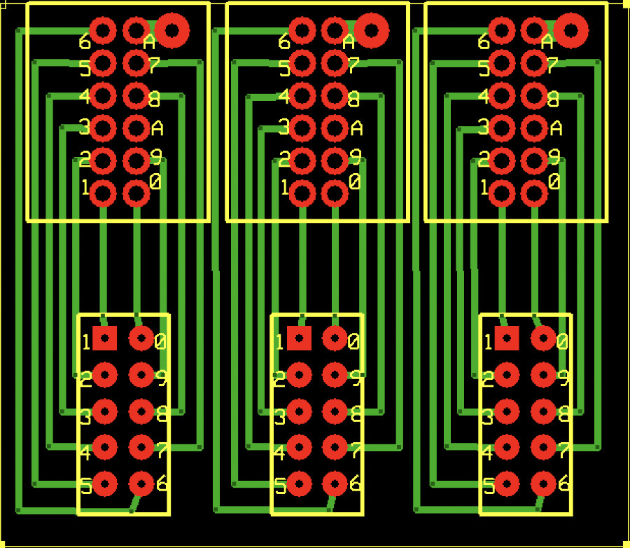
To the left are the 7441 nixie drivers. The nixies are mounted on the front panel well away from the Teensy, because the teensy had to be located in a remote part of the chassis to eliminate any issues with noise near the input signals which happen to be pretty close to the nixies. So 30 wires have to be soldered to the board and run to the nixie board shown later.
Below is the PCB that I designed for the Teensy 4.1 controller circuit. The ground plane and the power plane are not shown because they make it impossible to see the traces clearly. This design is sent to the PCB Express fab shop to be made into a real board.
The nixie board will hold the nixies and be mounted to the front chassis. It will obviously be a DIY board.
The teensy board needs small voltages, less than 3.3V, so I designed the board below to input the current and voltages from the amp. Off-board voltage dividers consisting of 470K and 1K resistors reduce the voltage to less than 3.3V and feed into J1. The voltage inputted into J1 = actualV * 1/(470 + 1).
This is a very safe voltage. Nevertheless, each signals is still sent through an op-amp and then onto a protection scheme consisting of a 470R resistor and 2 schottky diodes tied to +2.7V and to ground. Note that the negative voltages are sent through an inverting op amp first. This should pretty much guarantee that the teensy never sees a voltage higher than 3.3V, which would certainly fry it.
delta_kR and delta_kR are received from the Teensy board through J5, doubled by the op amps, and sent on to the meters. See explanation of delta_kL and delta_kR below.
Tpsu is brought on board, and Tamp is created on board and both were originally sent to op amps before going to Teensy board, but I have hard-wire bypassed the op amps now, because they weren't really necessary.
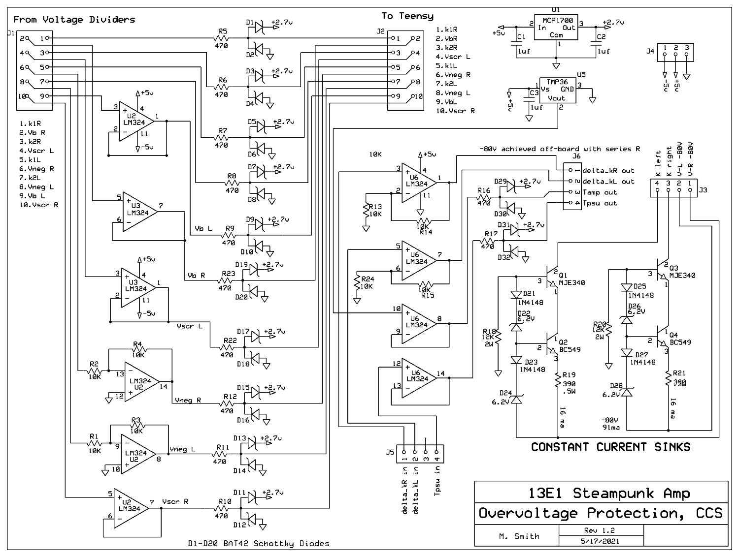
There was plenty of room left on the board, so I stuck the constant current sinks for the first stage on the same board. These are seen in the lower right corner.
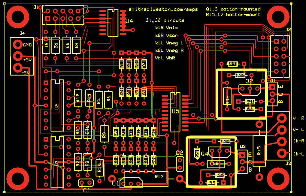
And below, of course, is the PCB design.
OVERCURRENT PROTECTION, METER BUFFERS, MOTOR DRIVERS
The Overcurrent Protection circuit below will shut down the entire amp if any of the cathode currents exceed about 200mA. The first line of defense is from the Teensy, which is monitoring the cathode voltages (currents) - it is connected to the SCR via pin 4 of J5 (KILL2). If Teensy detects any cathode current greater than, say, 200ma, it sends a LOGIC1 to the the C106 SCR U3, which then trips and pulls pin1 of J5 to ground. This activates the KILL relay on the PSU board and shuts down the transformer supplying the power tubes.
The backup, if the Teensy fails, is the circuitry shown at the top of the diagram. The maximum of K1R,K2R,K1L,K2L (taken from the cathodes of the 13E1's) is delivered to the base of Q1. When one of the cathode voltages reaches about 2V (200ma cathode current), Q1 is sufficiently turned on to trip the SCR.
The SCR stays permanently closed until all power is shut off and it resets.
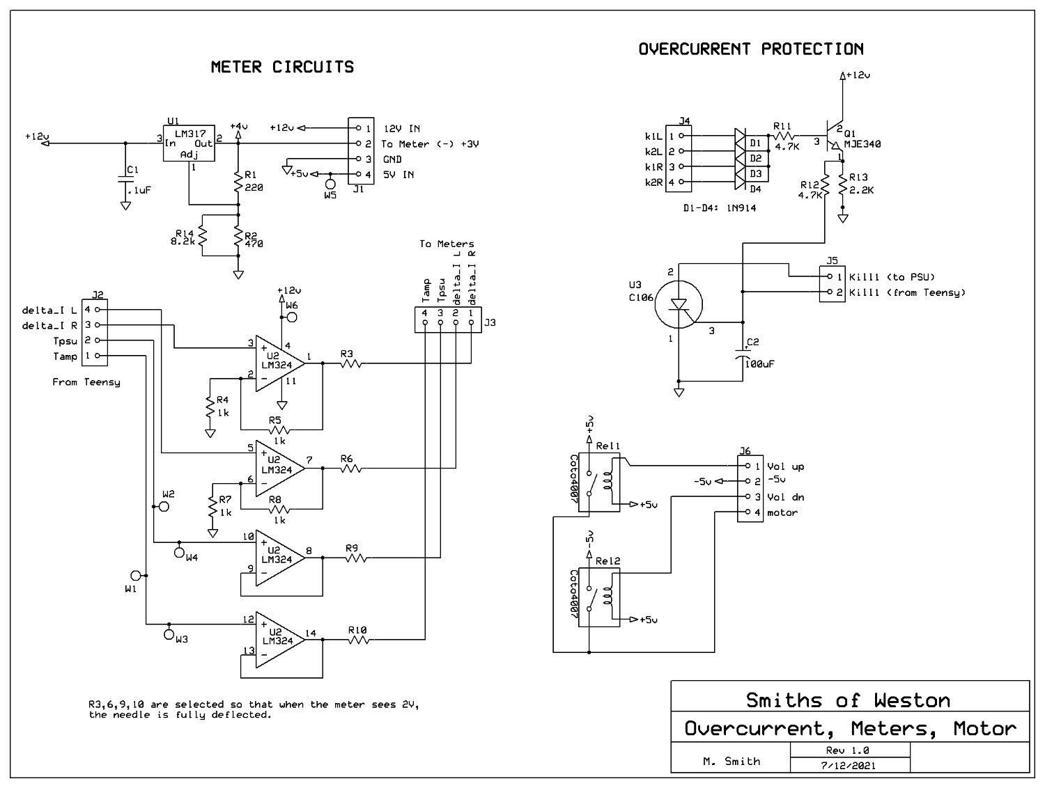
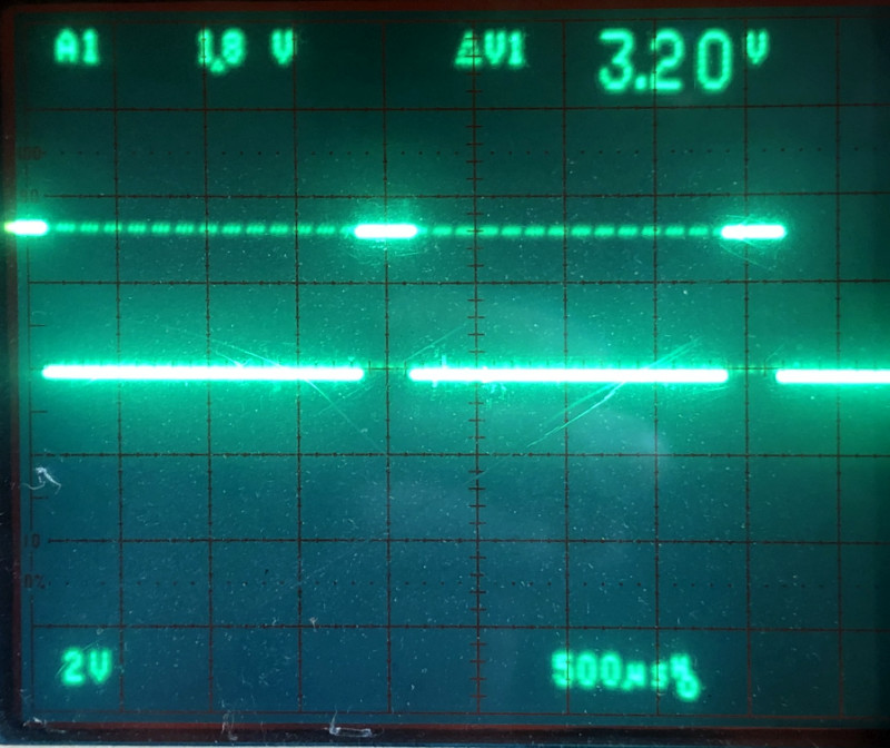
The meter buffers are simple op amps with an extremely low output impedance, so perfect for driving analog meters. The Teensy receives input from the temperature sensor and calculates the temperature. It then divides the temperature by 50 to convert it to a voltage suitable for output. e.g. if T=25C, .5V is outputted; if T=75C, 1.5V is outputted. The so that a 2V input causes full deflection of the needle (100C). Unfortunately, the Teensy cannot output an analog signal, so instead it outputs a pulse-wave modulated (PWM) signal. An example of this is below. This signal might be OK to send to the analog meters, but I have buffered it with a simple RC buffer. There are 4 such buffers made up of R12-15, C14-17 (see Teensy schematic above). This is sent to the meters. When T=25C, V=.25V and the needle is deflected 1/4 full-deflection. When T=75, V=1.5V, and the needle is deflected 3/4 full deflection.
The current difference (delta_k) signals are a little more complicated. The delta_k meters need to show negative values, as well as positive values. The Teensy obviously cannot output a negative voltage, so the following Smithlabs innovation (lol) is used:
The Arduino software is adjusted so that when the deltaI = 10ma, 2.5V (after buffering) is outputted, and when deltaI = -10ma, .5V is outputted, and when deltaI = 0, 1V is outputted. This is sent through the 2X amplifying op amp buffers shown above, so that when deltaI is 10ma, the meter gets 5V and when the deltaI = -10ma, the meter gets 1V.
If you put 3V on the ground pin of the meter, when the meter gets 5V on its positive terminal, it sees 2V across the terminals. When the meter gets 1V, it sees -2V across its terminals. R3 and R6 are adjusted so that +2V across the terminals causes full deflection to the right, and -2V causes full deflection to the left.
The little circuit on the bottom right is to drive the motor on the motorized Alps potentiometer (volume control). They require separate voltage regulators to provide +5V and -5V. My favorite little COTO PCB relays are perfect for this and have been used in all my other amps.
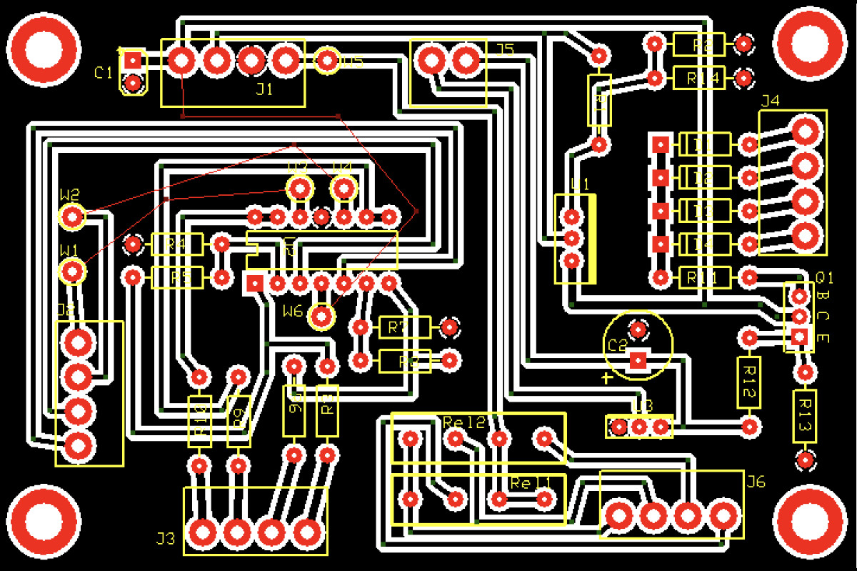
This little collection of circuits is just perfect for a handy-dandy DIY printed circuit board. It saves me the $85 to have 3 boards manufactured by the fabrication house. Look here for how these homemade PCB's are made right here at Smiths of Weston HOT labs. HOT = "hopelessly outdated technology." The PCB design is shown below. Everything black will be exposed copper. The yellow silkscreen layer will not be included.
POWER SUPPLY
The essential elements of the power supply are shown below. There are multiple outputs.
1. 430V DC to the left and right rails.
2. 250V DC (regulated) for the screens of both channels. This comes from 430V off the left transformer.
3. 170V for the nixie tubes. This comes from 430V off the right transformer which is reduced to 170V with a simple zener regulator.
4. -100V DC for the negative rail.
5. 6.3V for all the 6SN7 and EL84 filaments
6. 26V AC to the 13E1 filaments.
AC N comes directly from the wall plug, while AC L comes from a relay circuit, described below in the soft-start schematic.
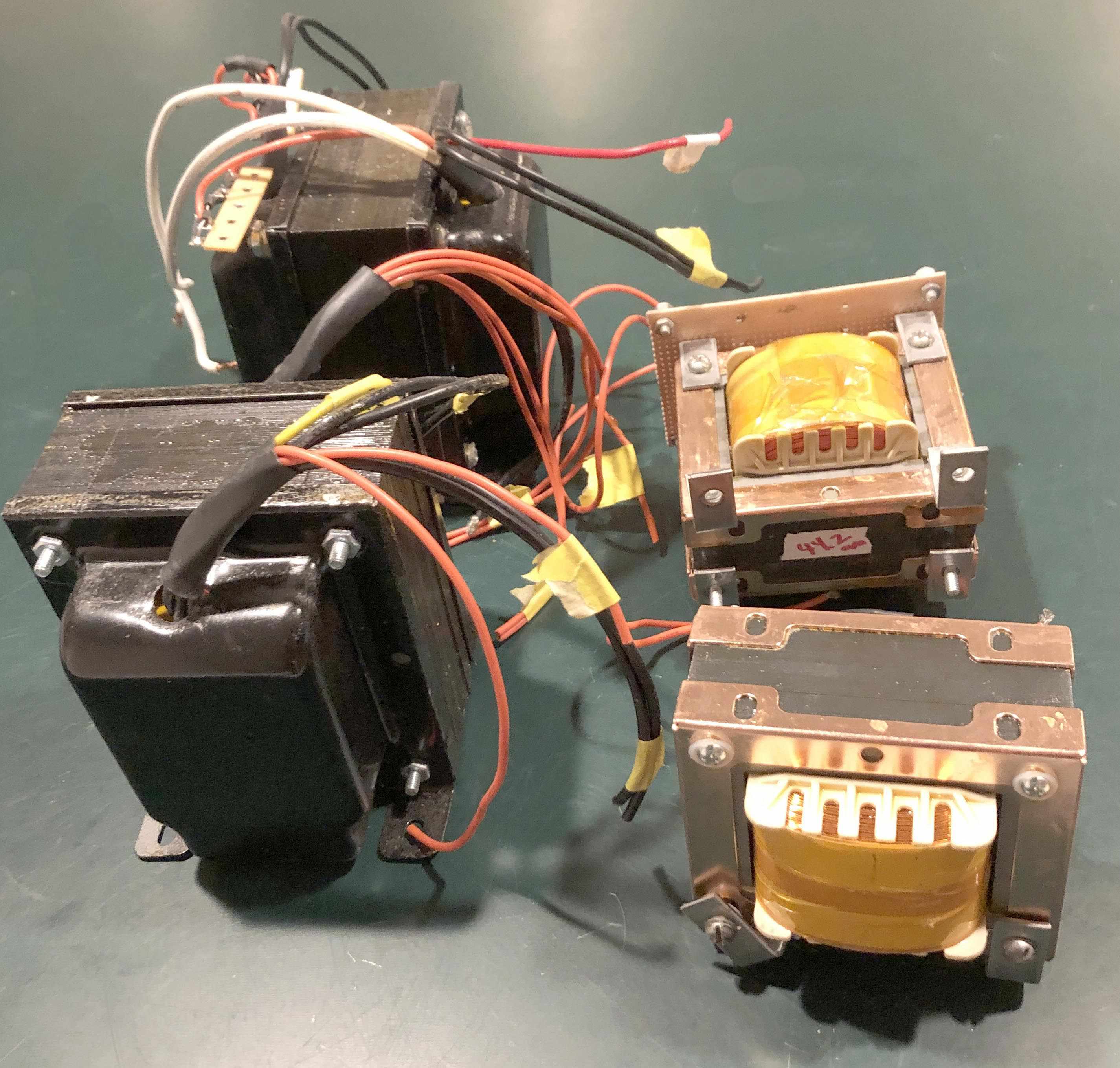
The power transformers were designed and wound by me and details are shown here. Originally, I used a choke for smoothing and designed and built 2 beautiful chokes. They are shown below, but will not be used.
The power supply worked beautifully, but it weighed a TON, so I abandoned the chokes and went with capacitor multipliers, as I have done with previous amplifiers. The layout of the power supply is shown below:
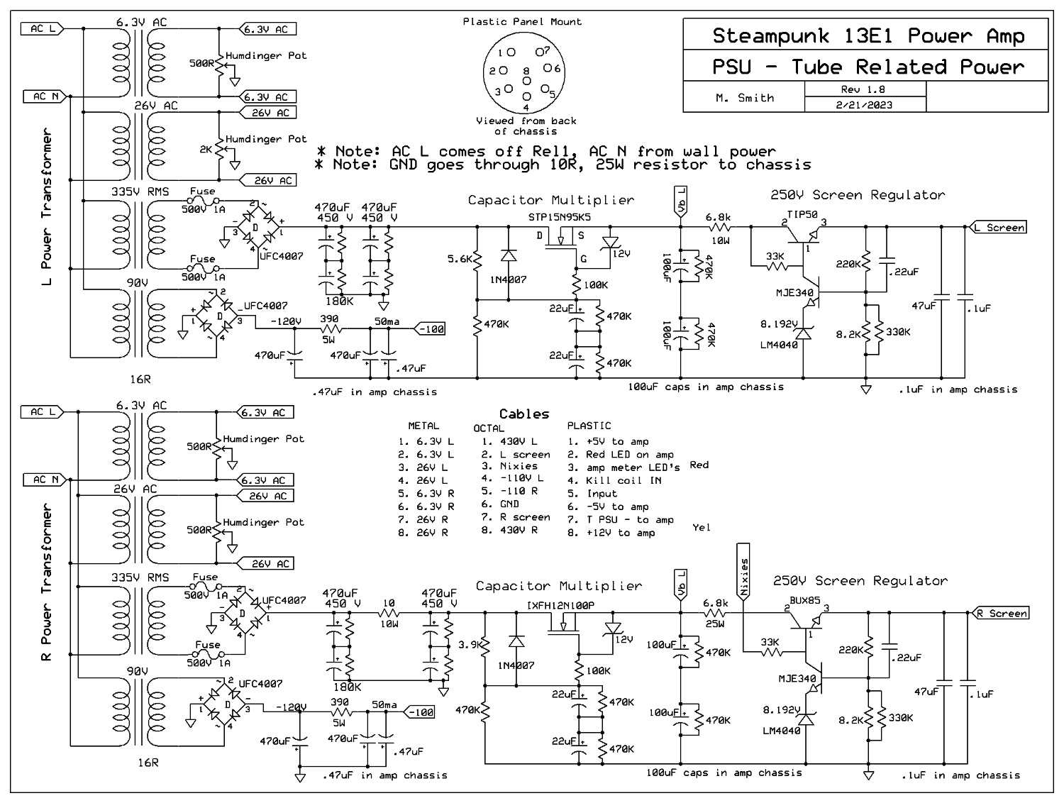
The capacitor multipliers work as follows: the raw voltage from the large capacitors is sent to the drain of the N-channel MOSFET. It also passes through a voltage divider consisting of 5.6K and 470K, which reduces the voltage slightly. This reduced voltage is sent into the gate of the MOSFET through a 100K stopper resistor. The current into the gate is negligible (picoAmps) so there is almost no ripple across the 11uF (22uF X 2 in series) capacitor. Because the MOSFET is in common source configuration, the source will attempt mightily to follow the gate, so since there is almost no ripple going into the gate, there is almost no ripple emerging from the source. The 5.6K resistor in the voltage divider is chosen so that it drops a voltage at least as high as the peak ripple voltage going into the gate. This works extremely well. There is a capacitor multiplier for each channel.
Each channel has its own negative supply, approximately -114V fully loaded.
Each channel has a 250V regulator to provide voltage to the screens. It is a very simple, classic 2-transistor regulator. The voltage across the 8.2K resistor = the sum of the voltage reference voltage and Vbe of the MJE340. This is in the neighborhood of 8.6V. So, there will always be around 1.1ma through the 8.2K resistor. So the voltage at the top of the 220K resistor = 1.1 * (220 + 8.2) = 251V.
The right channel 250V regulator also provides power to the nixies. Each nixie anode gets an anode resistor. The datasheet gives recommended anode resistance for a number of input voltages. It recommends 33K resistor for a 250V supply.
SOFT-START FUNCTION
Because of huge currents flowing into the PSU capacitors, a soft-start is required. This is accomplished with the setup shown below. When the amp is turned on, either with the remote or the hard switch, INPUT (from the Teensy board) goes LOW. This turns on Q5 and Q3, shutting off the Red LEDs on both the PSU and amplifier chassies, and turning on the amp meter lights, respectively. At the same time, Relay3 is energized and sends 12V into the soft-start circuitry.
The 12V energizes Rel1, which allows the line voltage to flow through the 3 10-ohm thyristors into the transformers.
Meanwhile, the 10uF capacitor C6 begins charging through R12. This slowly turns on the N-channel MOSFET Q1 which allows current to start flowing thru the coil on Relay2. So the voltage starts dropping at the source of Q1, and hence the base of Q2. When the voltage has dropped to about 11.3V, Veb approaches .7V which abruptly turns on Q2 and causes instant charging of C6, which instantly turns on Q1 and energizes the coil on Rel2. The resistors are arranged so that Rel2 is energized about 150msec after turn-on. When Rel2 is energized, the line voltages bypasses the thyristors, so the full line voltage is sent to the transformers.
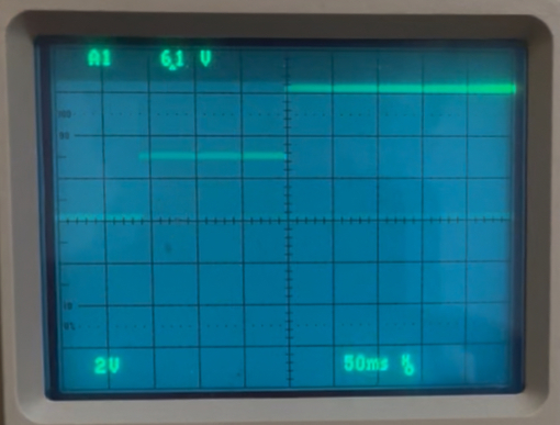
To confirm the timing of the soft-start, 5V was applied "Line in" on J4 and output measured by oscilloscope at "XFMR" on J4. A 30R resistor was placed on "XFMR" and taken to ground, forming a voltage divider with the 3-10R thyristors. "INPUT" was grounded, starting the soft-start. Relay1 is closed, and the voltage at "XFMR" immediately goes to 2.5V because of the voltage divider. After about 150msec (seen on the scope tracing), Relay2 closes, bypassing the thyristors, and 5V is measured at XFMR. This confirms that the soft-start circuits will delay full energizing of the transformers by 150msec.
Note that the line voltages go through the KILL relay which is kept on by Q4. In an emergency, "KILL in" goes low, shutting off Q4, which shuts off the KILL relay, and shuts down the power transformers. "KILL in" is controlled by the Teensy microcontroller and/or by a hardware protection circuit discussed later.
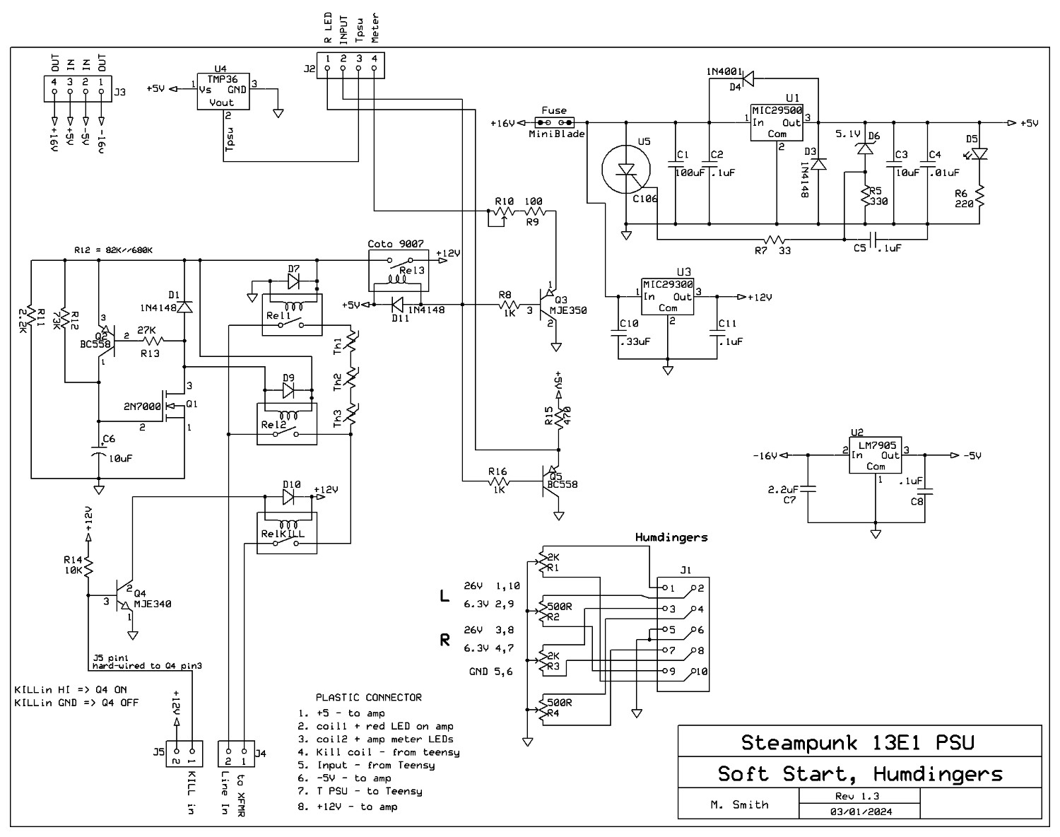
LOW-VOLTAGE REGULATORS: these are standard regulators. The 5V regulator is a high-current device and is heat-sinked. It is protected by an overvoltage crowbar circuit comprised of a C106 SCR, D6, R15, and R17. If the output voltage of the regulator goes above around 5.7V, .6V is presented to the SCR which turns it on. This shorts the input to ground and blows the fuse. I have lost many sensitive 5V parts in the past, and I hope this helps prevent some of those losses in the future.
HUMDINGERS - these are simply 500R trimpots placed between each pair of AC filament windings. They have worked extremely well in the past to make my amps dead quiet.
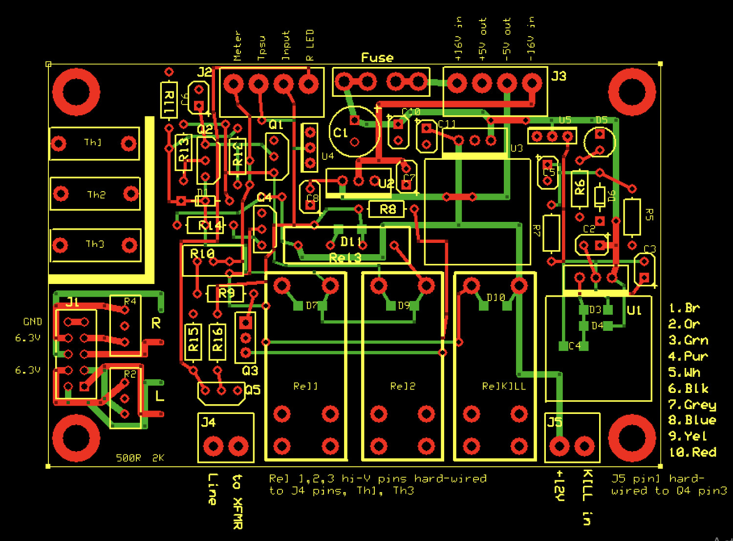
Below is the PCB board design.
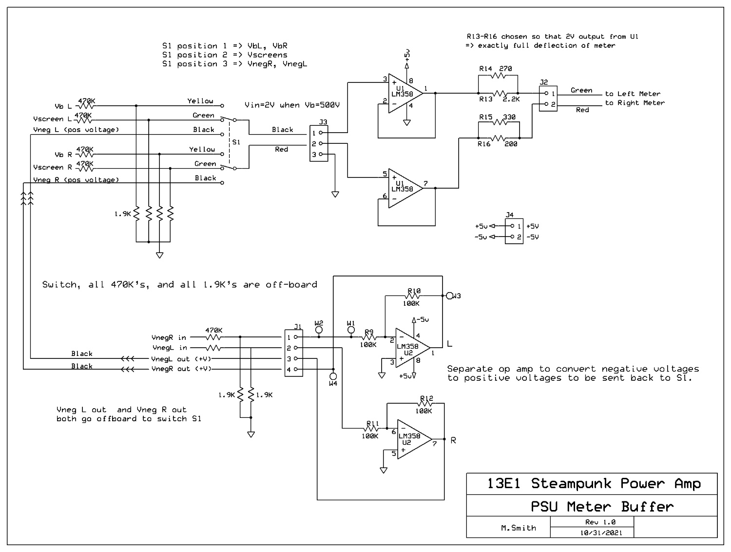
PSU CHASSIS ANALOG METER BUFFERS
The analog meters mounted on the front of the power supply are delicate D'Arsonval movement devices. Just as in the amp chassis, the high voltages need to be knocked down by a voltage divider. A 470K:1.9K divider gets the voltages down by a factor of about 250. The voltages selected by the switch pass to the LM358 op amps in U1 and then on to the meters. The negative voltages are similarly reduced by a voltage divider and are passed to the op amps in U2 where the polarity is reversed and they are doubled. These signals then pass off-board to the switch and pass through the switch just like the other positive voltages. R13-R16 are selected to perfectly calibrate each meter.
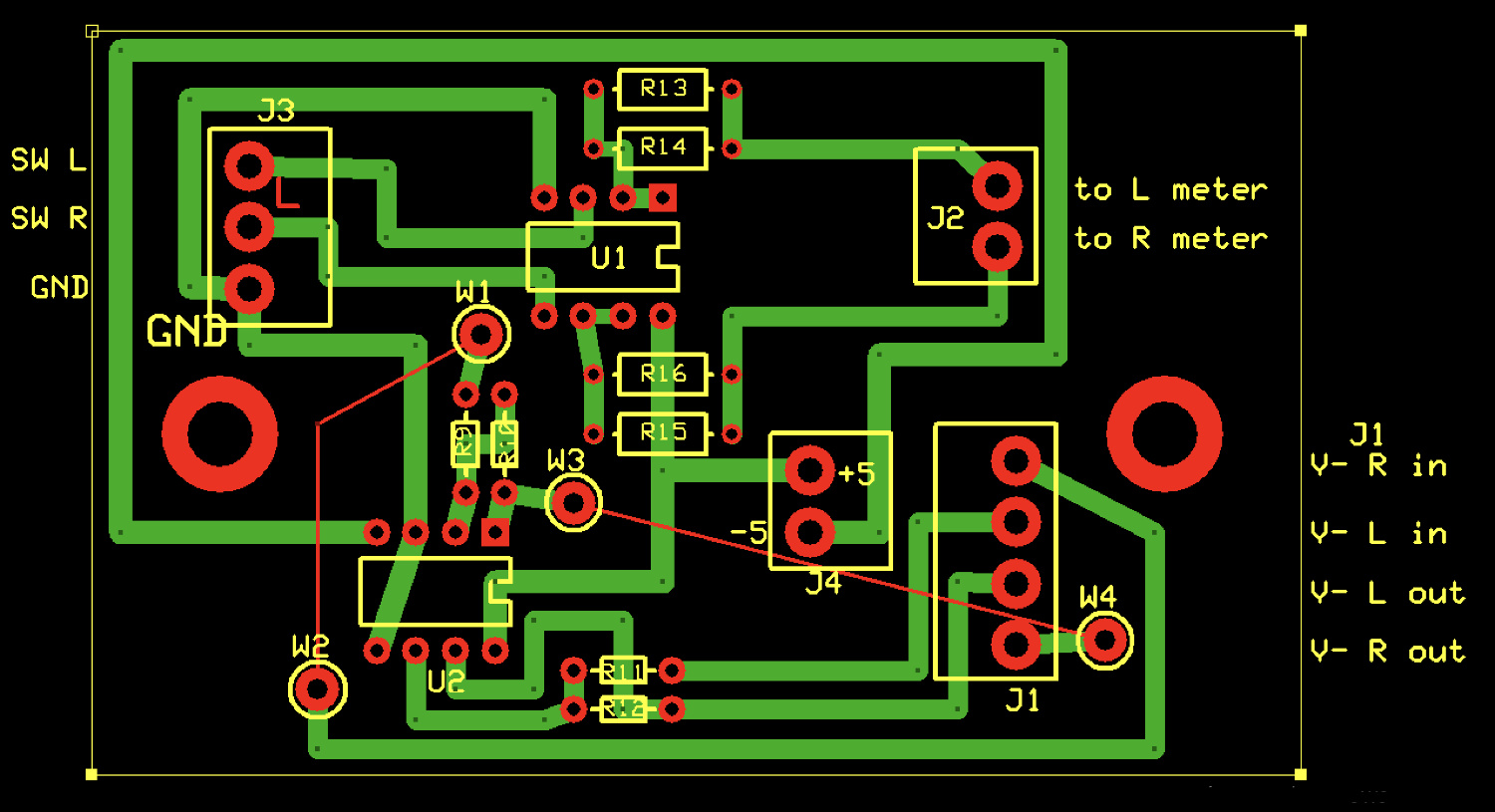
Below is the PCB board design. It is relatively simple, so I'll save $100 and DIY it.
SIGNAL SENSOR
The cathode current balance meters on the front of the amp chassis are extremely sensitive and jump all over the place while music is playing. This is annoying and I'd like to inactivate those meters when music is playing. I needed to find a simple signal sensor that would output a digital "1" when a signal was sensed and a "0" when no signal was detected. The digital 1 or 0 is sent to the Teensy. When a signal is present, the Teensy sets deltaIk = 0 for both channels. This places the needles midposition and motionless on the meters.
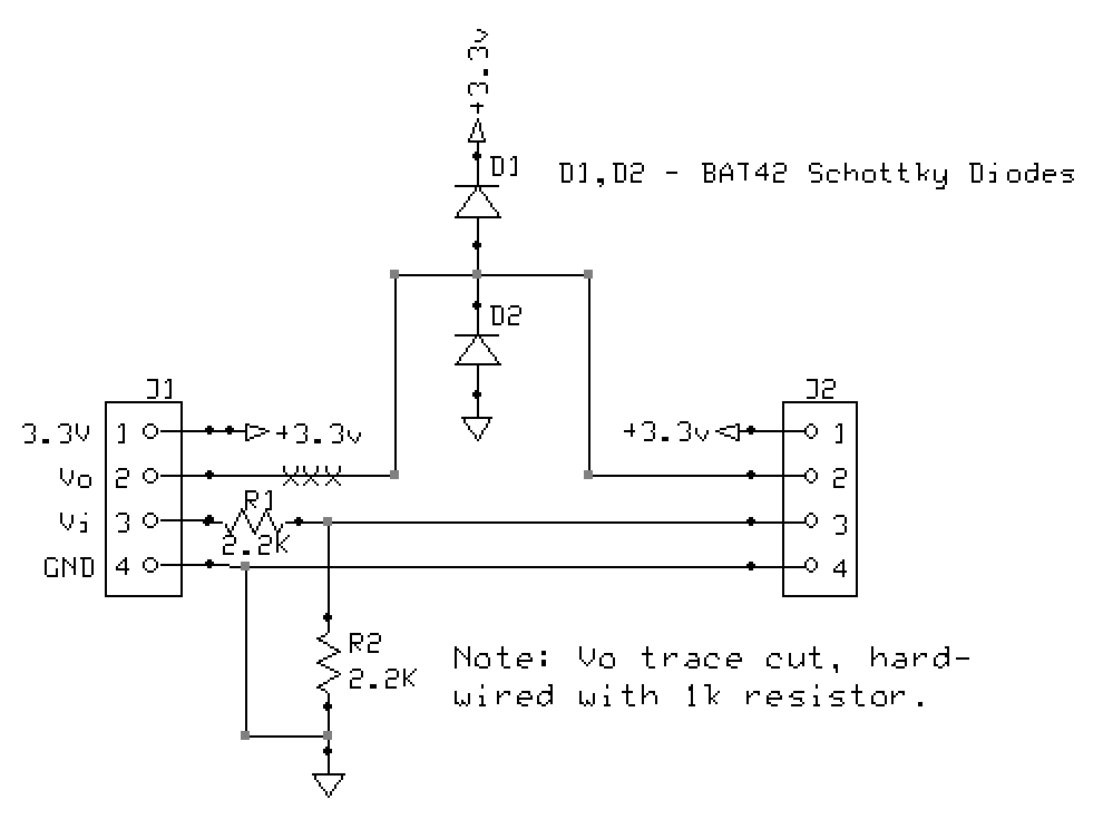
I found a little circuit on eBay (chinese, of course, lol) for $10 that does exactly that. I designed a little circuit board to hold the circuit.
Below is the schematic. The little circuit will fit into J2. The 2 resistors reduce the input which is taken off the right speaker jack. The 2 Schottky diodes prevent the output from exsceeding around 3V - this protects the Teensy microcontroller from excessive voltages. The input will fry if over 3.3V. After I made the printed circuit board, I realized that I forgot to include the 1K resistor on the output. This is hard-wired in. Below is the schematic and the PCB that I DIY'ed.
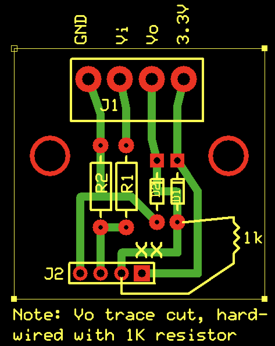
NOTE: after playing music at all volumes, I saw that the meters did not go crazy after all, so I disconnected this little circuit.
MEASUREMENTS AND FEEDBACK ADJUSTMENTS
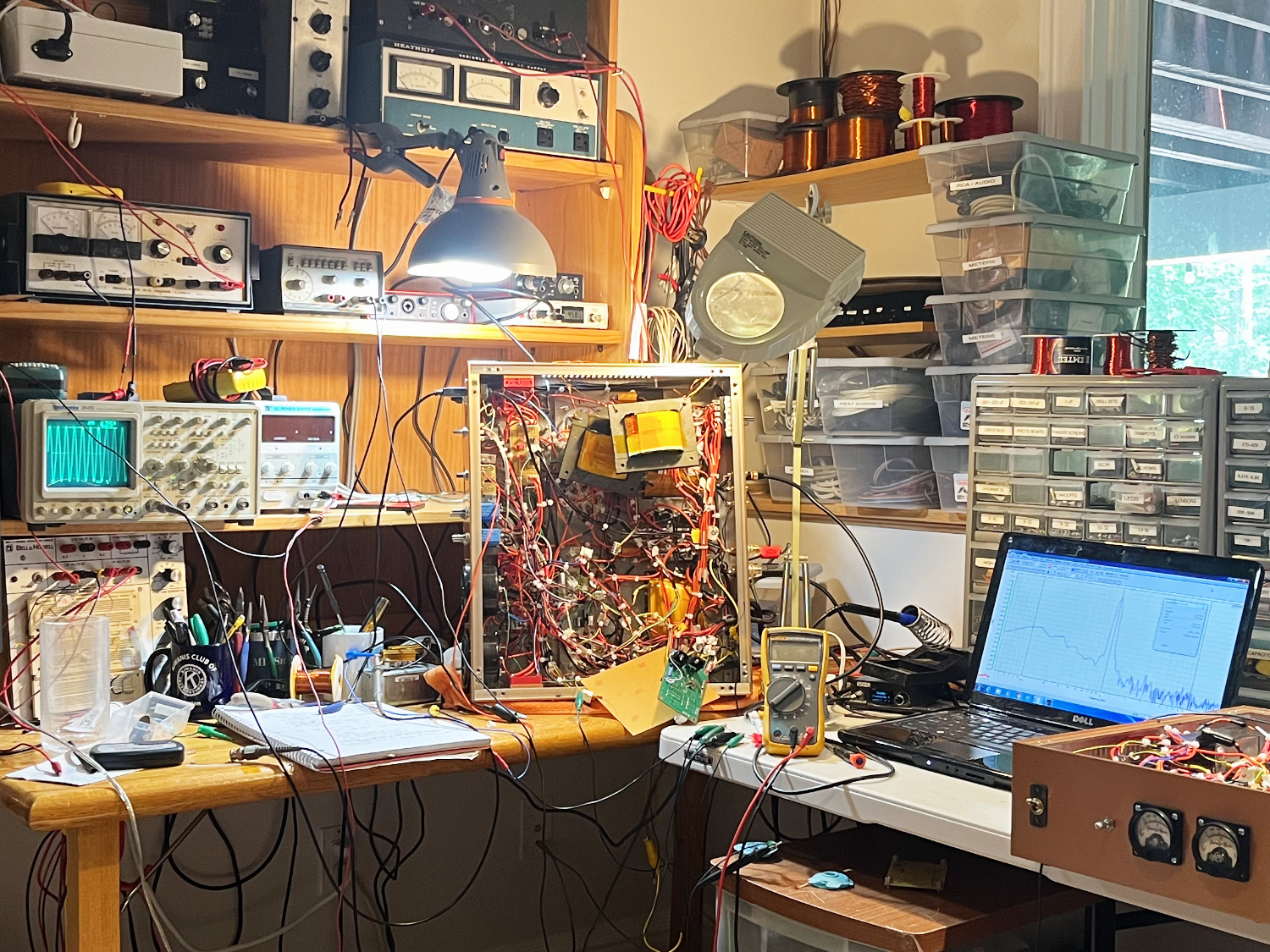
Below is the testing setup I used. Lots of ways to die doing this - do not use during cocktail hour. My old dependable analog scope is displaying the output at the speaker. The FFT (Fast Fourier Transform) seen on the old Dell computer is generated by Akulap, a very nice audio measurement program. My trusty Fluke multimeter is standing by. The anode chokes for the EL84's are hanging by wires to keep them out of the way. All the control circuitry, microcontroller, etc. are removed.
Transformer Impedance (Ra-a) Measurements
Knowing Ra-a is necessary in order to calculate the value of the resistor in the Zobel network on the transformer primary. This is discussed above in "Compensation Networks."
I applied 6.66 Vrms to the primary of the output transformer and measured the output at the speaker on both 4ohm and 8ohm settings:
4ohm: Vo = .176 Vrms. So turns ratio is .176/6.66 = .0264. So impedance ratio = .02642. So reflected impedance across the primary = Ra-a = 4 / .02642 = 5.7K.
8ohm: Vo = .236 Vrms. So turns ratio is .236/6.66 = .0354. So impedance ratio = .03542. So reflected impedance across the primary = Ra-a = 8 / .03542 = 6.4K.
Using a 6K 5W resistor is probably close enough.
Gain measurements
Gain was measured with and without global negative feedback (GNF), and with 4ohm and 8ohm speaker settings.
A = gain without GNF, A' = with GNF. GFB = 20log(A/A').
R channel 8 ohm: A = 45.8, A' = 11.66 => GFB = 11.9 dB.
L channel 8 ohm: A = 42.6, A' = 11.44 => GFB = 11.4dB.
R channel 4 ohm: A = 33.6 , A' = 10.52 => GFB = 10.1dB.
L channel 4 ohm: A = 31.4 , A' = 10.29 => GFB = 9.7dB.
Note that the right channel gain is a little bigger than the left channel gain. I will leave these as is and will probably not notice when I do listening tests. If I do notice, I will make some adjustments to even up the gains
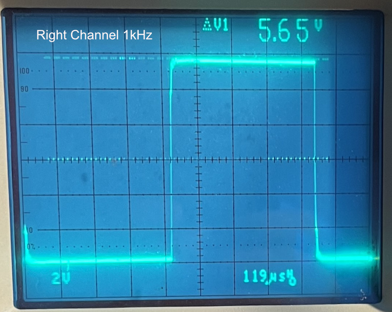
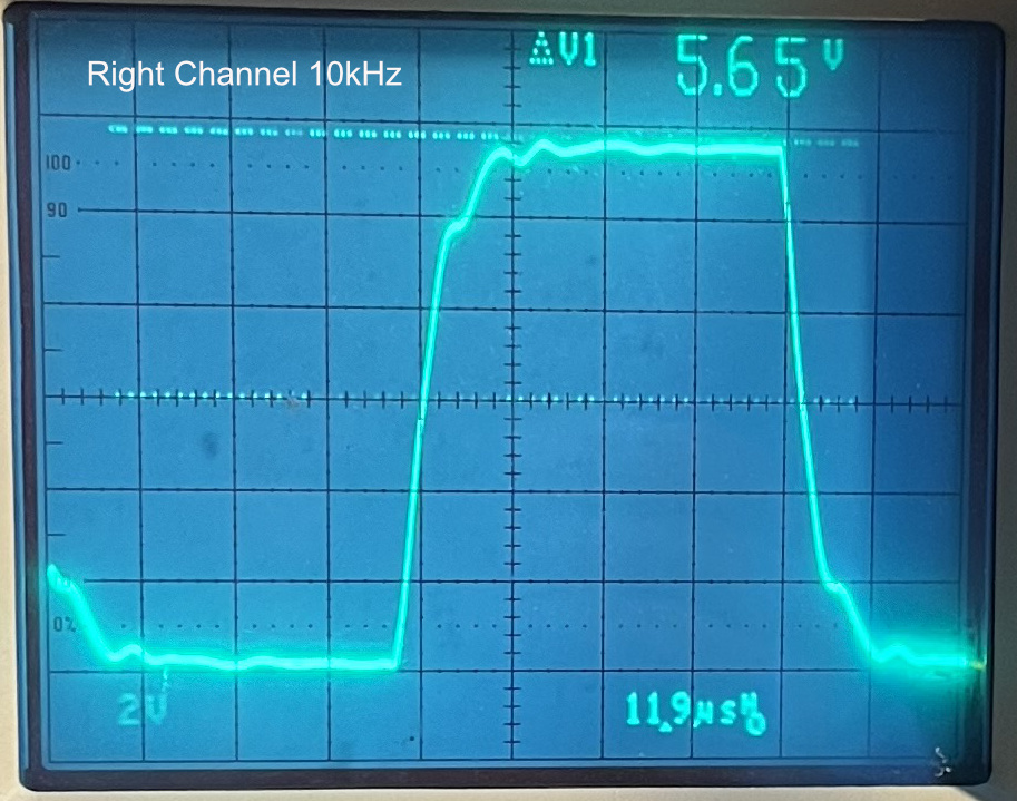
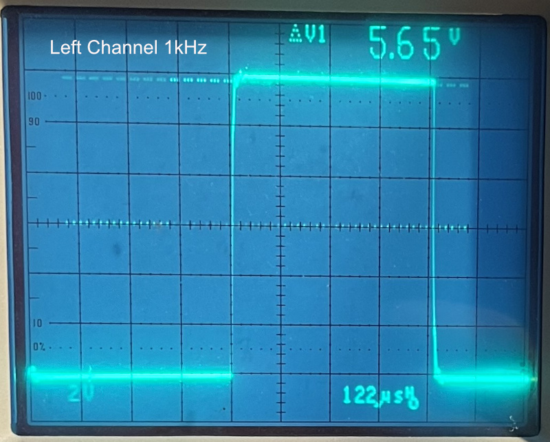
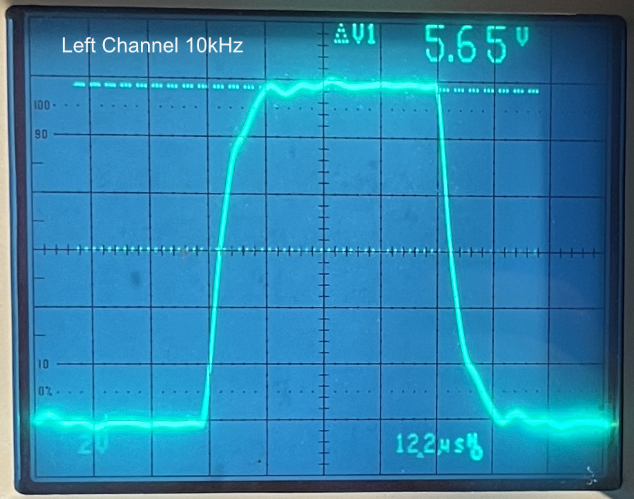
Square Wave Testing
This is done to test the susceptibility of the amp to oscillation.
Output Impedance
LEFT
4ohm setting: 1.6ohm without GNF, 0.7ohm with GNF.
8ohm setting: 0.5ohm without GNF, 0.2ohm with GNF.
RIGHT
4ohm setting: 1.4ohm without GNF, 0.4ohm with GNF.
8ohm setting: 0.4ohm without GNF, 0.2ohm with GNF.
CONSTRUCTION STEPS
The chassis was manufactured by Landfall Systems in Austin. A custom chassis like this is outrageously expensive - way more than most amplifiers on the market. I had a separate chassis made for the amp itself and for the power supply
The filament (heater) wiring is done first. 18ga red and black wire is used throughout and twisted as tightly as possible. This reduces (hopefully eliminates) the irritating hum that accompanies many tube amps. Note the layout around the edges. This is to keep it away from the input signal which is low voltage and very susceptible to picking up the AC hum.
I had already wired the screens on the power tubes when I took this picture.
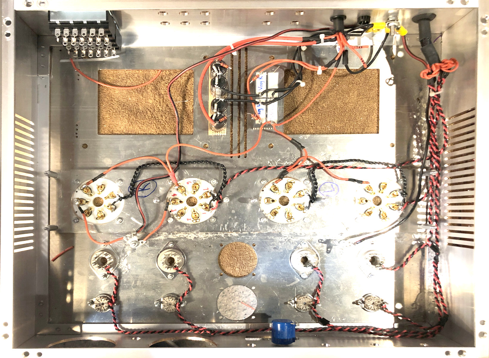
The next step is to wire the power tubes, the 6SN7 input tubes, and the EL84 driver tubes. The RCA jacks are wired and the electric ALPs potentiometer is installed and wired. The speaker jacks are wired also. The coupling capacitors are the red rectangular components. The wiring has not been organized yet, so is a bit messy appearing.
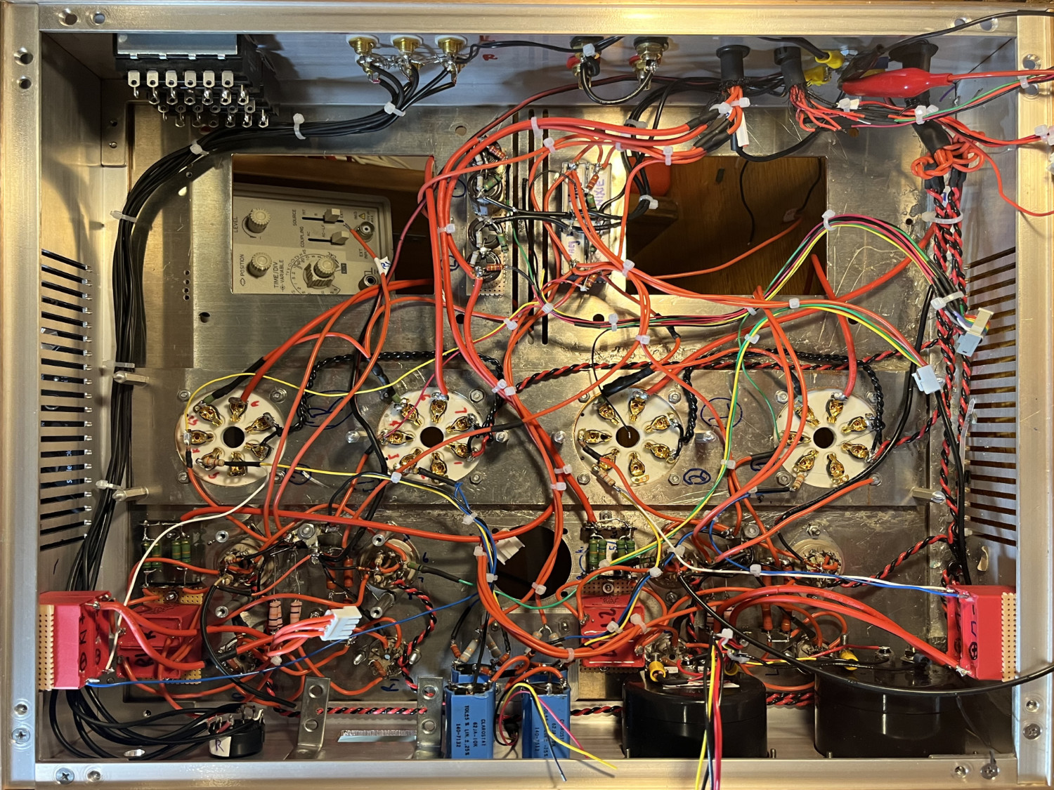
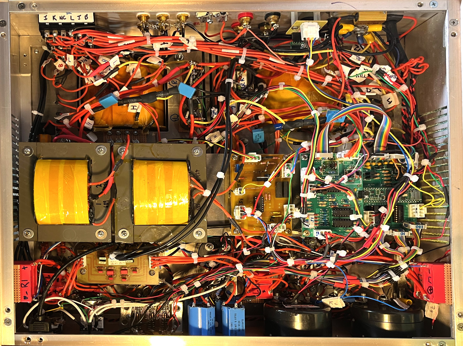
The next step is to build and install the output transformers. Actually, since I didn't take any pictures during the construction process, the next step is to build the entire amp. This is shown below. The wiring looks extremely complex, because it is. The nixies required 12 wires each. The wiring for the speaker switches was also extremely complicated. Everything is labeled, and I have all the schematics and the PCB layouts stored, so it is actually fairly easy to work on. I know, because I have made numerous changes during this process.
AMPLIFIER TESTING
I started using a new (for me) soundcard-based audio analyzer called REW (Room Equalization Wizard). It was created to analyze acoustics in rooms, but it can also be used to analyze amplifier performance. The amazing thing is that it is freeware, created by an old dude name John Mulcahy. It is so good that many professional audio equipment manufacturers use it. I hope they clicked the "donate" button. I contributed $50.
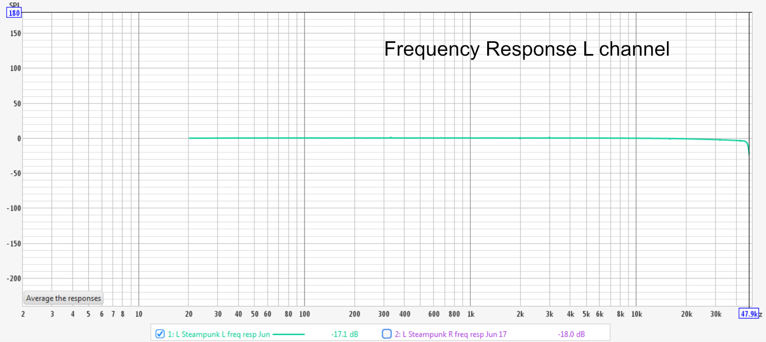
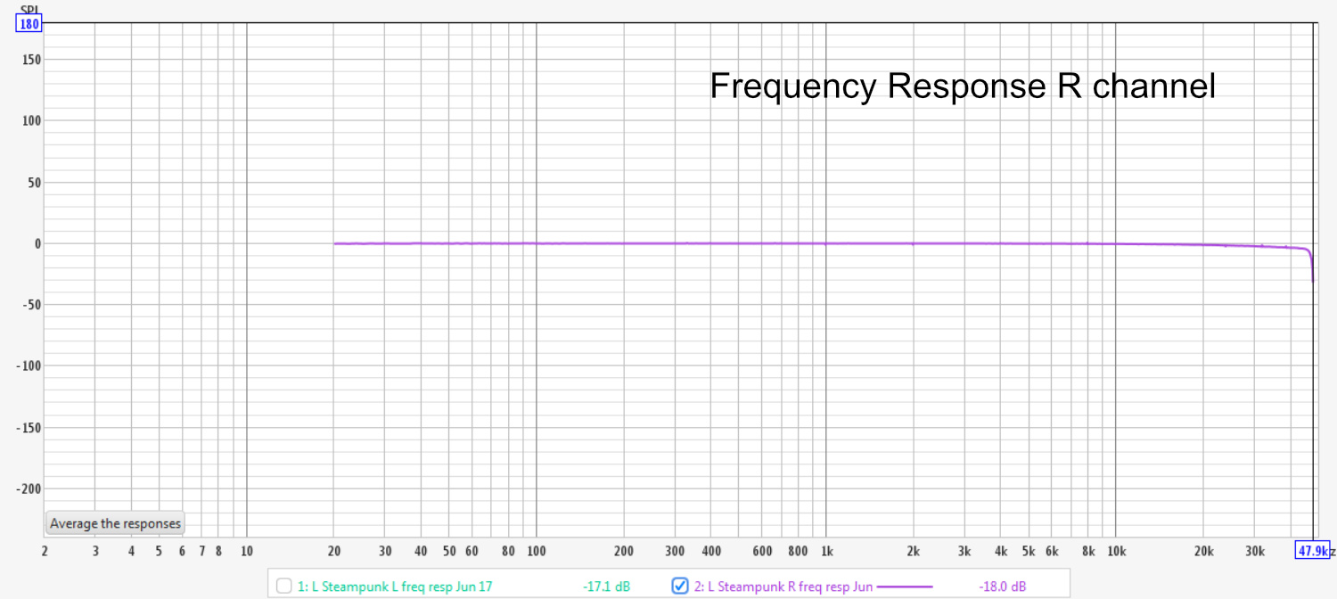
First, I did a frequency response test for both channels - shown below. They are dead flat and identical. So far, so good.
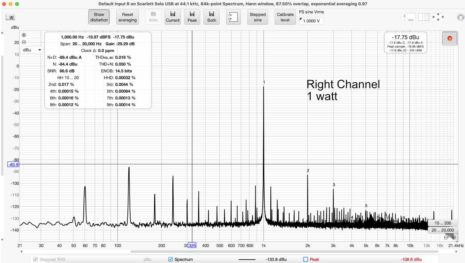
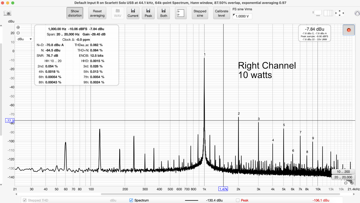
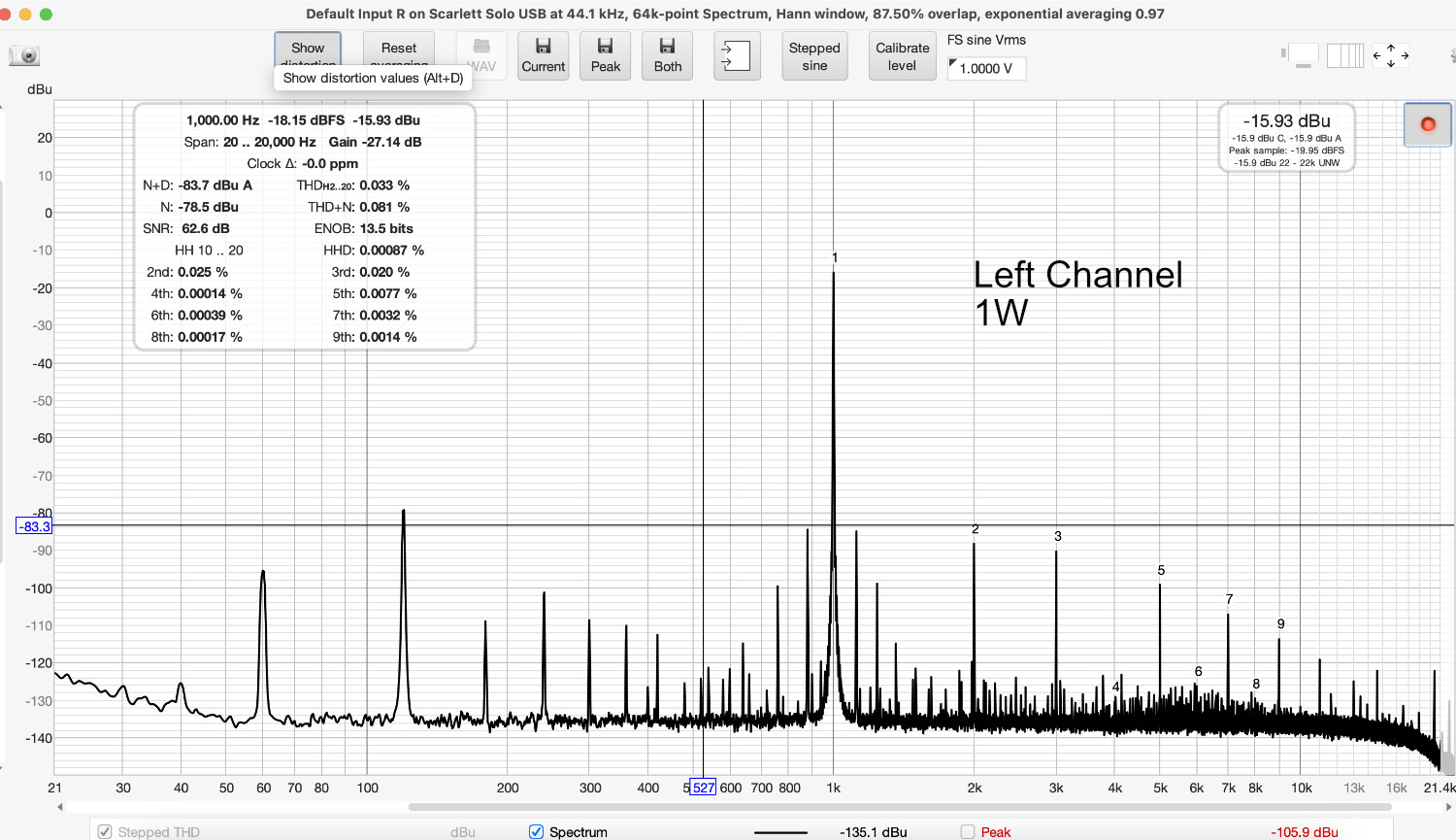
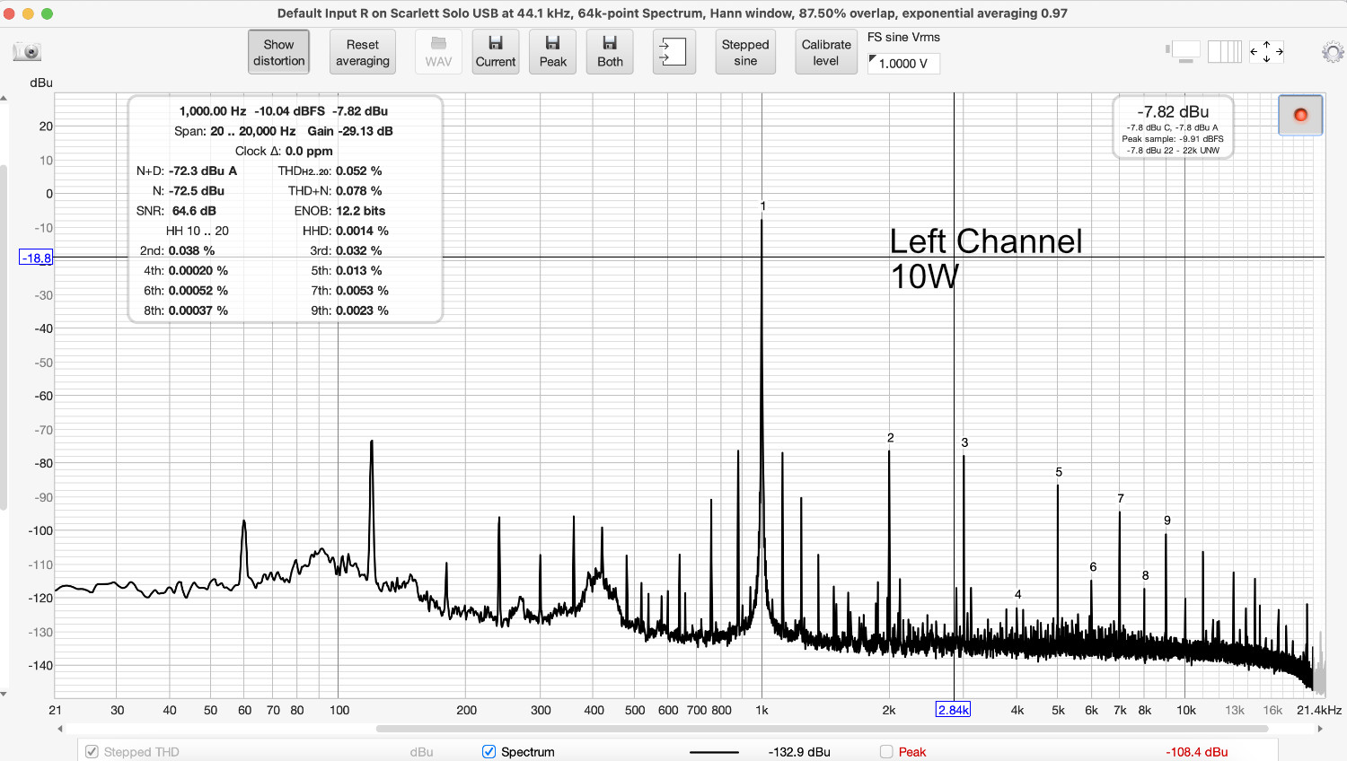
The following FFT's (fast fourier transforms) were done for both channels, at 1W and 10W. They show harmonics up to the 9th harmonic.The distortion figures are shown in the upper left portion and are pretty amazing. A full distortion analysis is shown later.
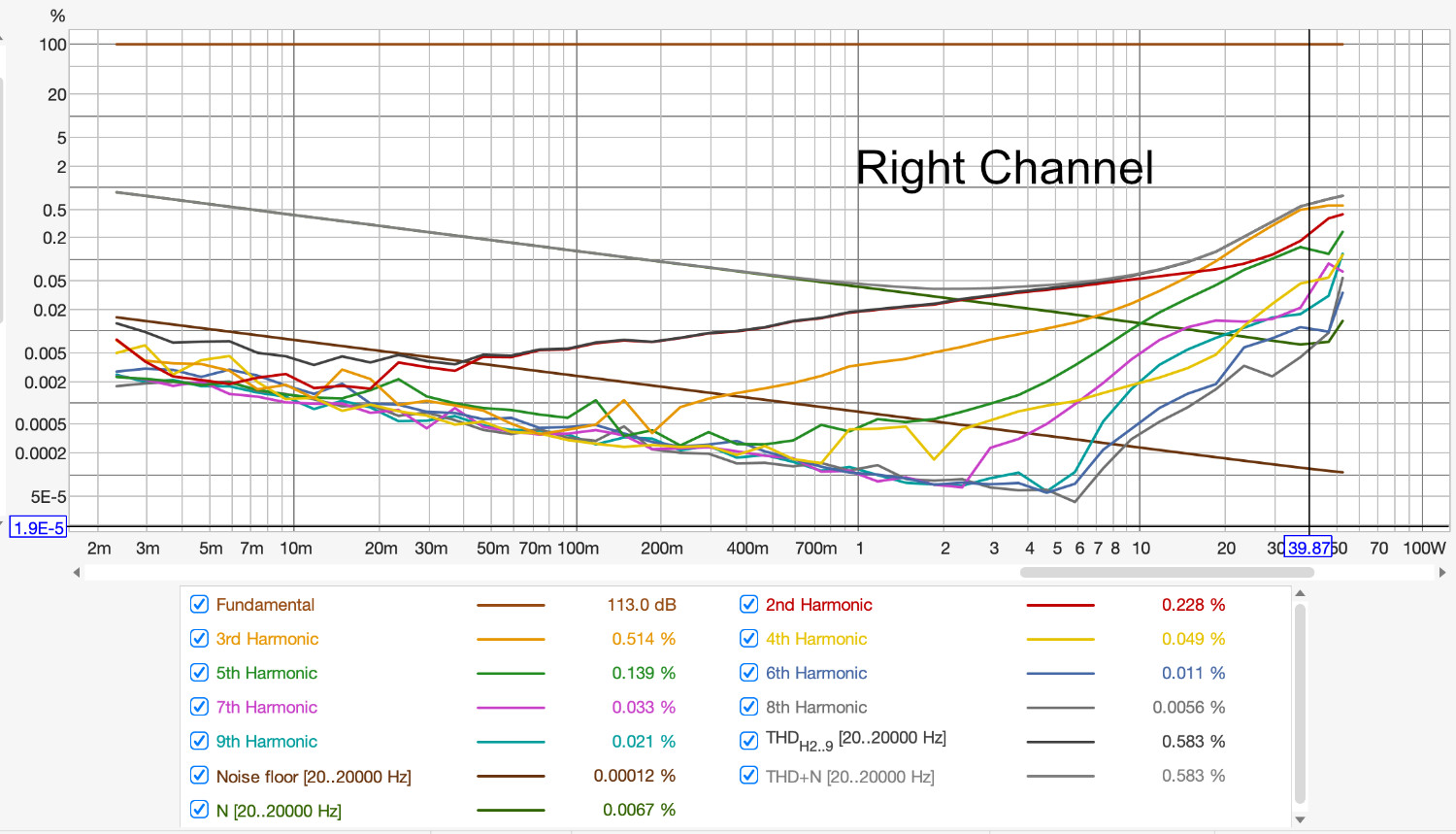
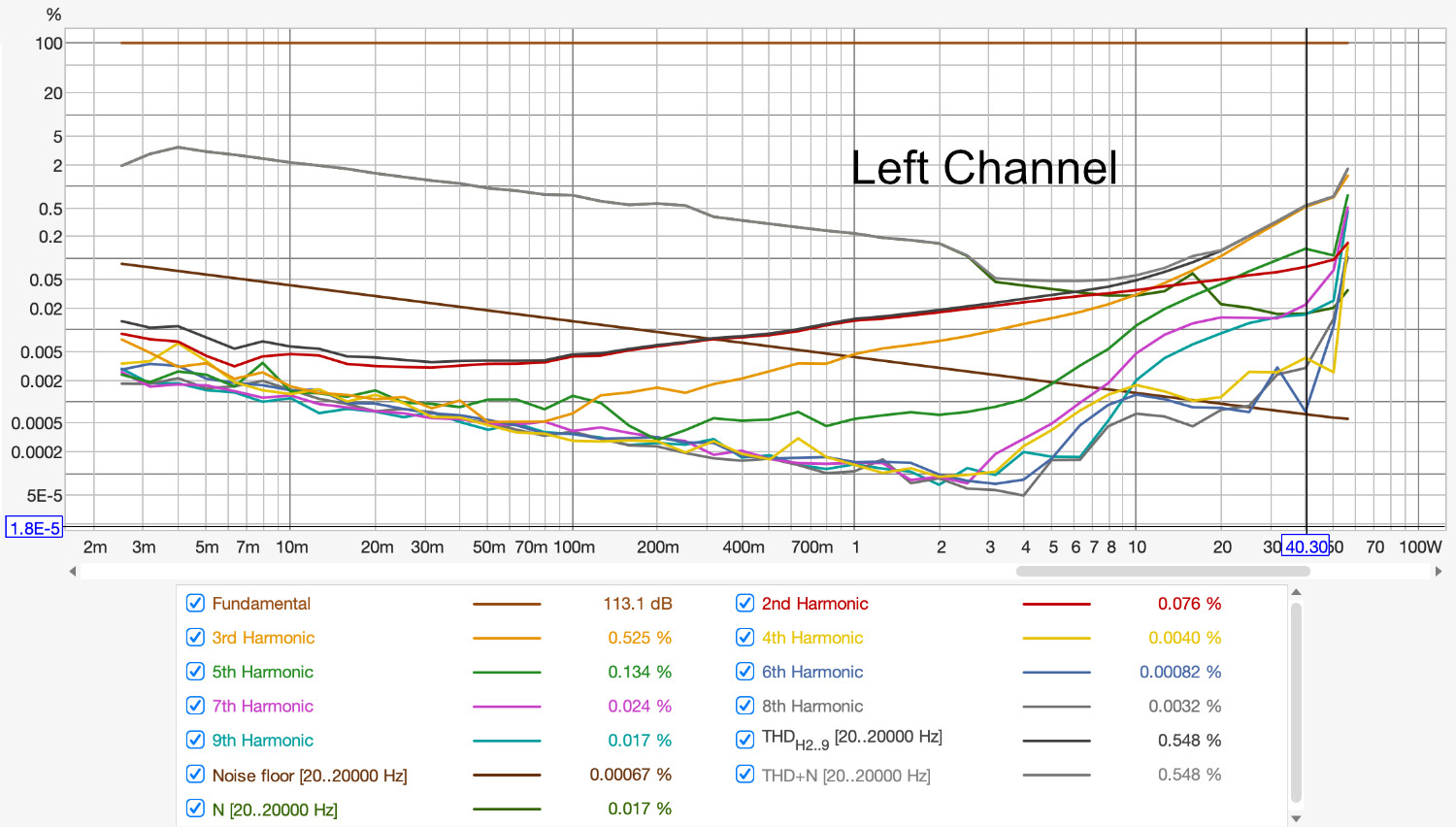
A full "stepped THD" distortion analysis was then done from 0 to 50W. The output in the REW program is interactive, meaning that you click on a point along the x-axis (watts) and the distortion number are shown. I did a screenshot showing the results at 40W, which is ear-splitting volume through my efficient speakers. The amp is getting fairly close to clipping at 45-50W, so the distortion numbers start to shoot up. The left channel numbers are a little better than the right (2nd harmonic distortion of .076% vs .228%), but .228% is not noticeable when your ears are bleeding
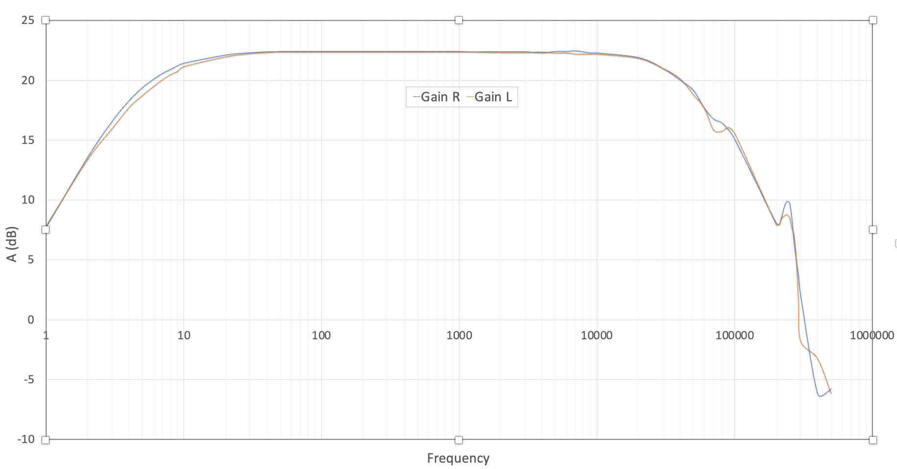
I manually measured gain for each channel from 1 to 500kHz, and plotted the values in Excel. The results for both channels are shown below. The curves are dead flat in the audio range. Everything looks pretty normal except for a little weirdness between 200-300kHz.
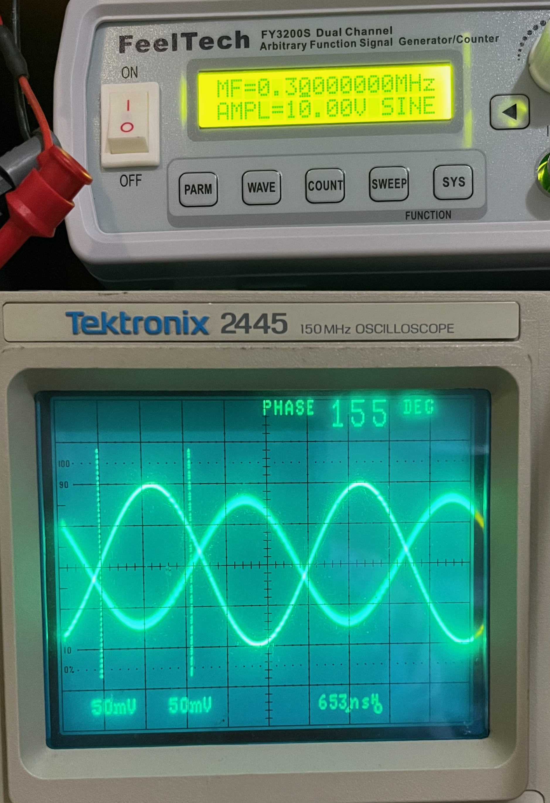
Using the phase shift measuring tool on my 40 year old analog oscilloscope, I measured phase shift for frequencies from 1 to 500khz. At no point was the phase shift > 180 degrees. The measurement shown below was done at 300kHz. The larger-amplitude signal is the input signal, which has been attenuated drastically at this high frequency. The smaller-amplitude signal is the amplifier output, and it lags the input signal by about 155degrees. Beyond this frequency, the gain was even smaller, so no chance of oscillation...I think. I repeated the measurements for the right channel, and the phase shift was 165 degrees, still safe.
Below are the square wave tests at 2W. I forgot to record the square wave tests without the compensation networks added, but they were extremely ragged with a ton of fling on the leading edge.